Electronic component device

Active Publication Date: 2020-04-09
MURATA MFG CO LTD
View PDF0 Cites 0 Cited by
  • Summary
  • Abstract
  • Description
  • Claims
  • Application Information

AI Technical Summary

Benefits of technology

[0074]As illustrated in FIG. 3, the first base body 211 and the second base body 221 may be in direct contact with each other with no bonding layer interposed therebetween, and the first base body 211 and the third base body 231 may be in direct contact with each other with no bonding layer interposed therebetween. In this case as well, advantageous effects of the present invention can be sufficiently obtained. Similarly, providing no gap between the second base body 221 and the third base body 231 does not impede the advantageous effects of the present invention.
[0075]The electronic component device 1 according to the present preferred embodiment includes the first mount board 11, the second mount board 12 positioned to face the first mount board 11 and electrically connected with the first mount board 11, and three or more electronic components including the first, second, and third electronic components 21, 22, and 23 disposed between the first mount board 11 and the second mount board 12. The first electronic component 21 is disposed on the first mount board 11, and includes a first major surface and a second major surface that face away from each other. The second electronic component 22 is disposed on the second mount board 12, and includes a third major surface and a fourth major surface that face away from each other. The third electronic component 23 is disposed on the second mount board 12, and includes a fifth major surface and a sixth major surface that face away from each other. The first major surface of the first electronic component 21 is positioned closer to the first mount board 11 than the second major surface of the first electronic component 21. The third major surface of the second electronic component 22 is positioned closer to the second mount board 12 than the fourth major surface of the second electronic component 22. The fifth major surface of the third electronic component 23 is positioned closer to the second mount board 12 than the sixth major surface of the third electronic component 23. The second major surface of the first electronic component 21 is in contact with the fourth major surface of the second electronic component 22 and the sixth major surface of the third electronic component 23, either directly or indirectly with the bonding layer 40 interposed therebetween.
[0076]The above-described configuration according to the present preferred embodiment can provide an electronic component device that has a greater number of paths through which heat can be dissipated (heat dissipation paths) than an electronic component device according to a comparative example. The reason for this will be described below.
[0077]FIG. 13 is a cross-sectional view of an electronic component device 100 according to a comparative example, schematically illustrating dissipation paths for heat generated in an electronic component 122. In the electronic component device 100, an electronic component 121 and the electronic component 122 are disposed between a mount board 111 and a mount board 112. The electro

Problems solved by technology

However, if heat can be dissipated through only the two heat dissipation paths mentioned above, he

Method used


Image

  • Electronic component device
  • Electronic component device
  • Electronic component device

Examples


embodiment

PREFERRED EMBODIMENT

1. BASIC STRUCTURE

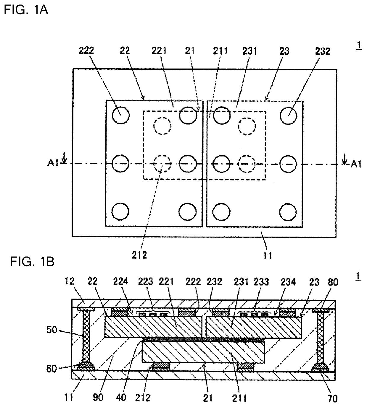
[0058]FIGS. 1A and 1B illustrate the structure of an electronic component device (module) 1 according to a preferred embodiment of the present invention. FIG. 1A is a plan view of the electronic component device 1. FIG. 1B is a cross-sectional view taken along an arrowed line A1-A1 in FIG. 1A.

[0059]In the following, for convenience of description, an electronic component 21 will be referred to as “first electronic component”, an electronic component 22 will be referred to as “second electronic component”, and an electronic component 23 will be referred to as “third electronic component”.

[0060]As illustrated in the plan view of FIG. 1A, the electronic component device 1 includes the first electronic component 21, the second electronic component 22, and the third electronic component 23. As will be described later, the first electronic component 21 includes a first base body 211, and a first outer terminal 212, which is an outer terminal of the first

example 1

A. Example 1

[0081]First, the following describes, as an electronic component device according to an Example 1 of a preferred embodiment of the present invention, an electronic component device in which at least two electronic components among the first electronic component 21, the second electronic component 22, and the third electronic component 23 are acoustic wave components or semiconductor components. Example 1 represents a case with a restriction placed on the type of each electronic component provided in the electronic component device 1 according to the basic structure. Accordingly, the same reference signs as those used for the electronic component device 1 according to the basic structure will be used in the following description.

I. First Aspect

[0082]In an electronic component device according to a first aspect of the Example 1, the first electronic component 21 is a semiconductor component, and the second electronic component 22 and the third electronic component 23 are acou

example 2

B. Example 2

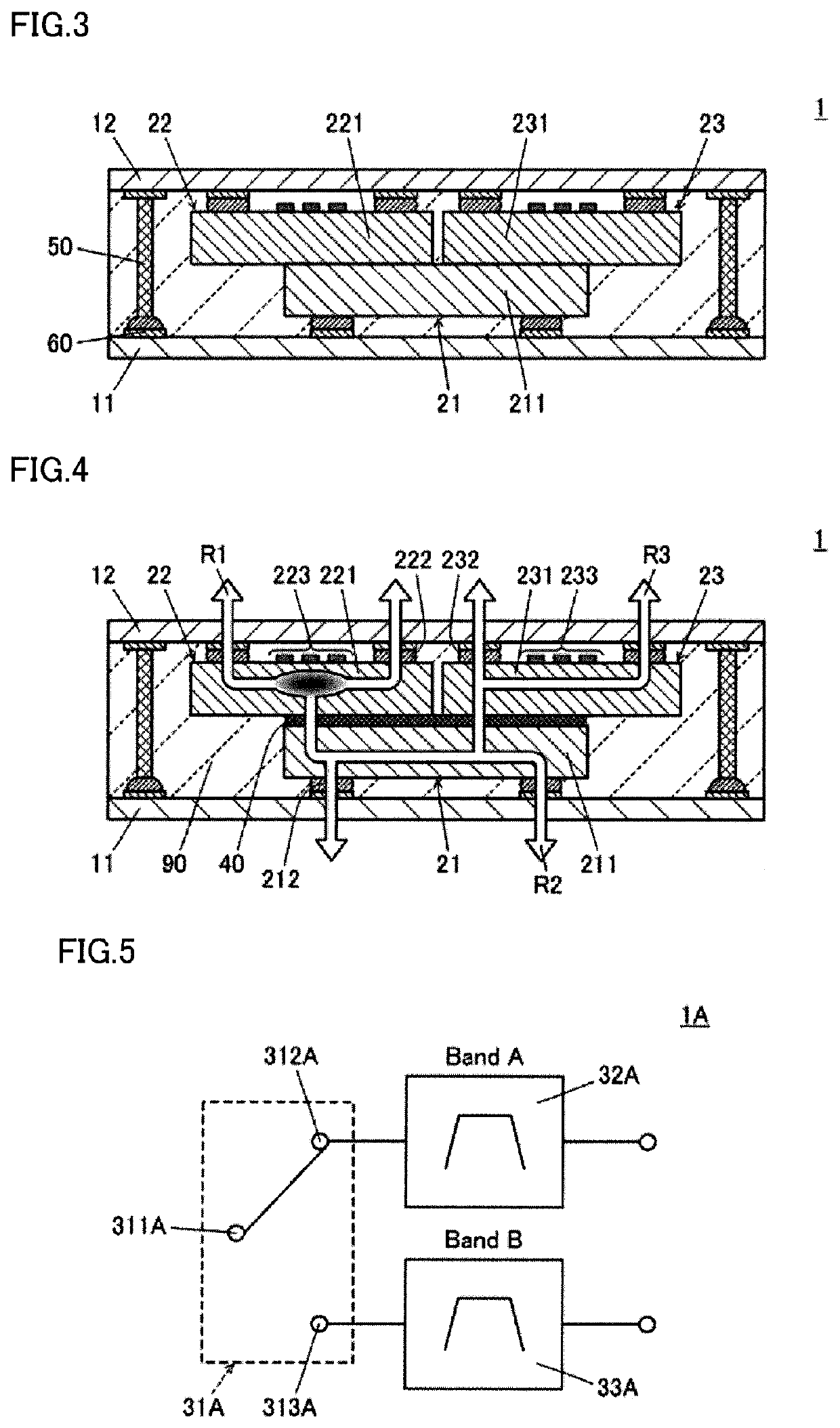
[0093]The following describes, with reference to FIGS. 5 to 10, an electronic component device according to an Example 2 in which the first electronic component 21 is a switching component and the second electronic component 22 and the third electronic component 23 are filter components. The aspects of Example 2 described below each represent an example in which the electronic component device 1 according to the basic structure is an electronic component device 1A, 1B, 1C, or 1D including a switching function and a filter function.

I. First Aspect

[0094]First, an electronic component device 1A according to a first aspect of the Example 2 will be described with reference to FIGS. 5 and 6. The electronic component device 1A according to the first aspect has a switching function to perform switching for two filter components among three electronic components that define an aggregate.

[0095]FIG. 5 is a circuit diagram illustrating a circuit provided in the electronic component dev


PUM


Abstract

An electronic component device includes first and second mount boards, and first, second, and third electronic components. The first electronic component includes a first major surface and a second major surface, and is disposed on the first mount board. The first major surface is positioned closer to the first mount board than the second major surface. The second electronic component includes a third major surface and a fourth major surface, and is disposed on the second mount board. The third major surface is positioned closer to the second mount board than the fourth major surface. The third electronic component includes a fifth major surface and a sixth major surface, and is disposed on the second mount board. The fifth major surface is positioned closer to the second mount board than the sixth major surface. The second major surface directly contacts the fourth and sixth major surfaces, or indirectly contacts the fourth and sixth major surfaces with a bonding layer interposed therebetween.

Description


Claims


Application Information

Patent Timeline
Owner MURATA MFG CO LTD
Why Eureka
Try Eureka