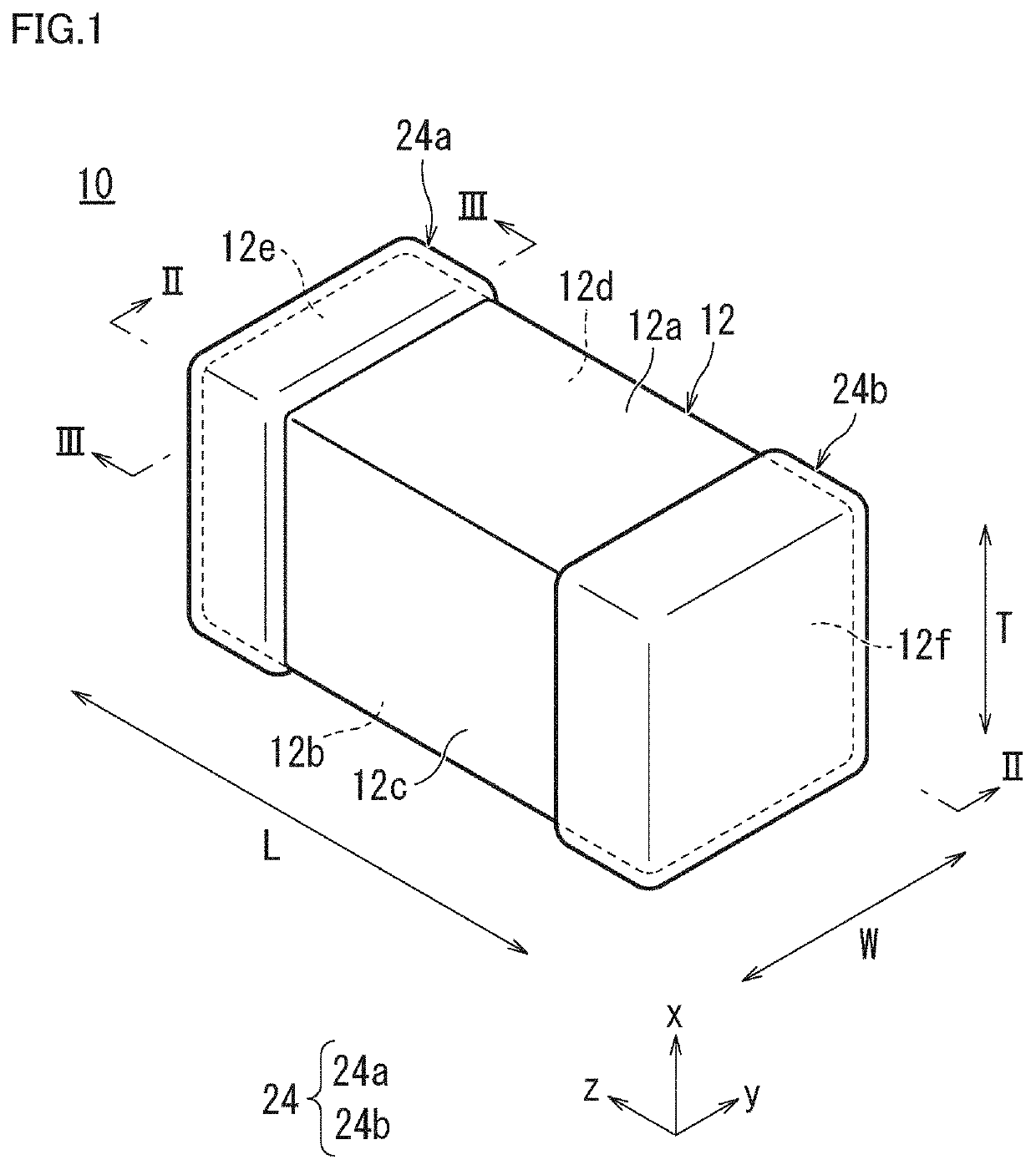
Multilayer ceramic capacitor
a multi-layer ceramic and capacitor technology, applied in the direction of fixed capacitors, stacked capacitors, fixed capacitor details, etc., can solve the problem of prone to delamination of multi-layer ceramic capacitors
- Summary
- Abstract
- Description
- Claims
- Application Information
AI Technical Summary
Benefits of technology
Problems solved by technology
Method used
Image

Examples
experimental example
3. Experimental Example
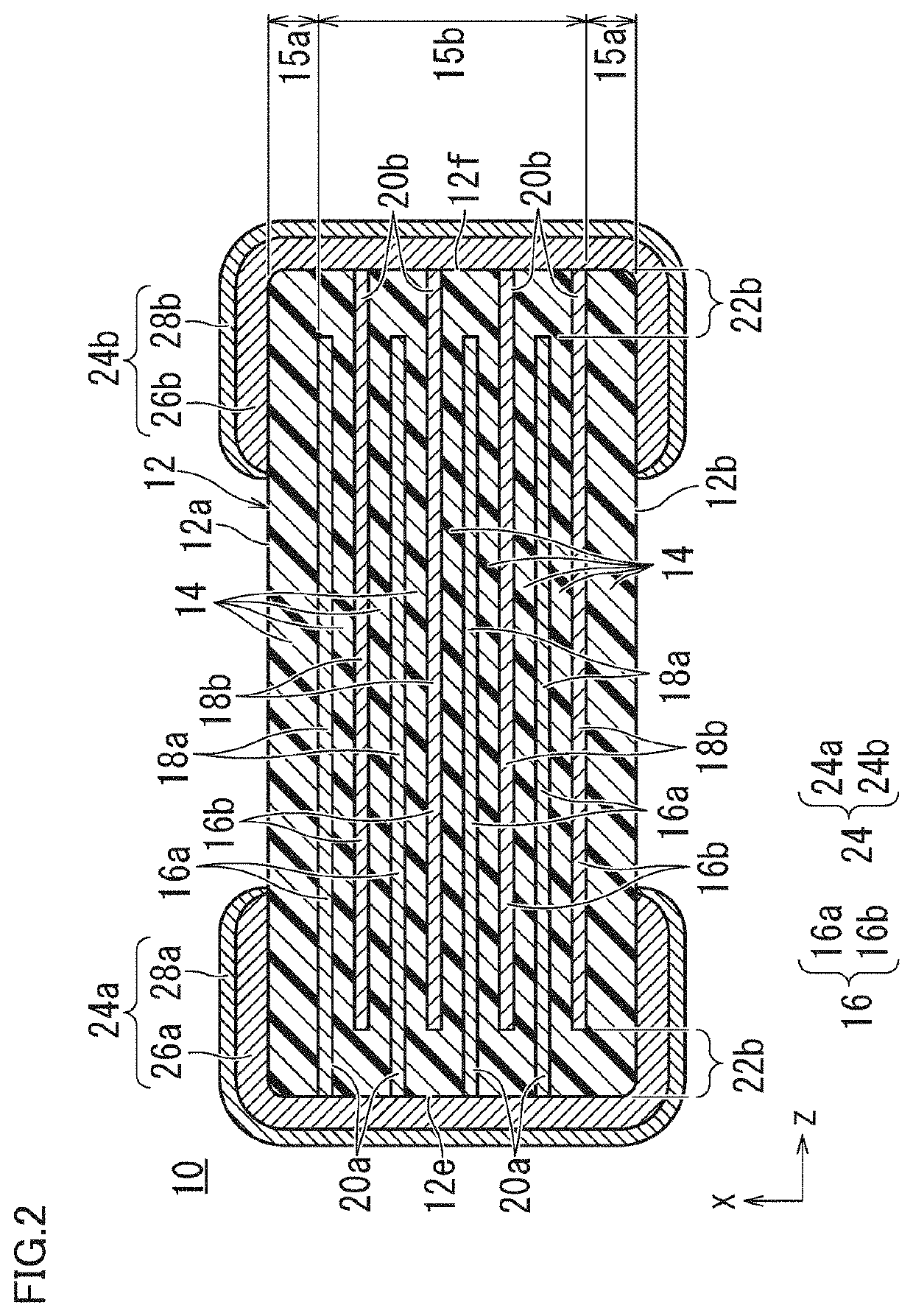
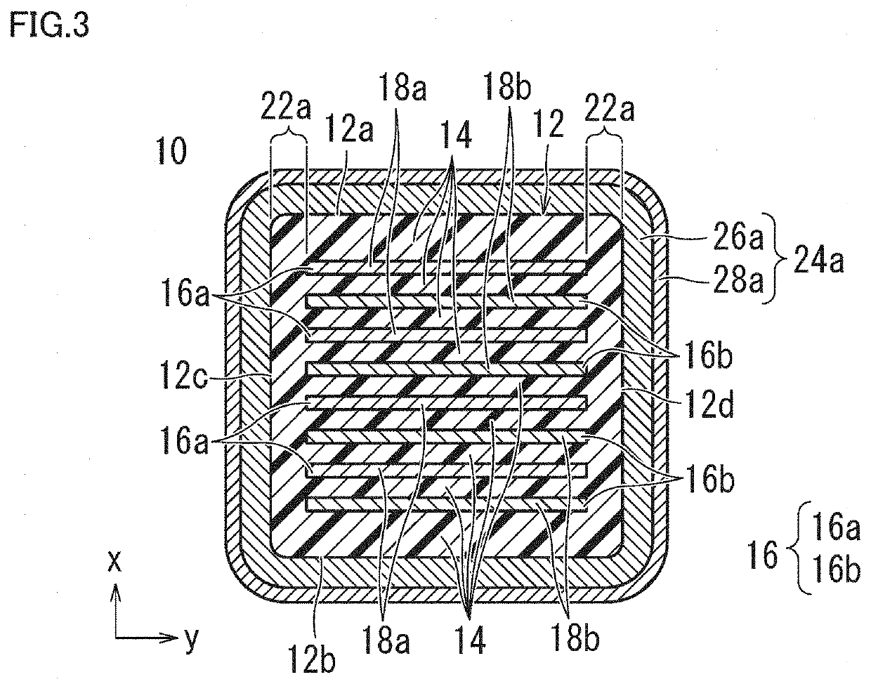
[0136]Next, in order to confirm the advantageous effects of the multilayer ceramic capacitor according to the preferred embodiment of the present invention described above, the multilayer ceramic capacitor was fabricated, and the capacitance was measured and a structural defect was confirmed.
[0137]Note that, in Experimental Example, the baked layer is provided as the underlying electrode layer.
(1) Specifications of Sample in Example
[0138]Multilayer ceramic capacitor size L*W*T (including the design value): length*width*height=about 3.25 mm*about 1.65 mm*about 1.65 mm[0139]Dielectric layer: CaZrO3 [0140]Thickness of dielectric layer: about 2.5 μm[0141]Inner electrode layer: Ni
Conditions of Inner Electrode Layer Formation
[0142]In the example of the above-described preferred embodiment of the present invention, the changes in coverage in the respective regions were controlled by changing the print pattern (the image line portion) for the portion of the inner electro
PUM
| Property | Measurement | Unit |
|---|---|---|
| Fraction | aaaaa | aaaaa |
| Fraction | aaaaa | aaaaa |
| Fraction | aaaaa | aaaaa |
Abstract
Description
Claims
Application Information
 - R&D Engineer
- R&D Manager
- IP Professional
- Industry Leading Data Capabilities
- Powerful AI technology
- Patent DNA Extraction
Browse by: Latest US Patents, China's latest patents, Technical Efficacy Thesaurus, Application Domain, Technology Topic.
© 2024 PatSnap. All rights reserved.Legal|Privacy policy|Modern Slavery Act Transparency Statement|Sitemap