Composite electronic component and board having the same

a technology of electronic components and composites, applied in the direction of printed circuit non-printed electric components association, sustainable manufacturing/processing, final product manufacturing, etc., can solve the problems of user discomfort, specific research into the degree of removal of acoustic noise, and the thickness of a ceramic chip disposed on a lower portion of a multi-layer ceramic capacitor. achieve the effect of decreasing acoustic nois

Inactive Publication Date: 2019-02-28
SAMSUNG ELECTRO MECHANICS CO LTD
View PDF7 Cites 4 Cited by
  • Summary
  • Abstract
  • Description
  • Claims
  • Application Information

AI Technical Summary

Benefits of technology

The invention relates to an improved way to reduce sound from electronic components that generate sounds. This can be done by adding materials or structures into certain areas on the circuit board itself.

Problems solved by technology

This patent describes a problem where users can hear loud noises caused by electronic components installed within electronic devices. Existing solutions involve reducing the amount of space needed for these components, but they cannot fully eliminate this issue. Additionally, there is a desire to reduce the number of components required without compromising their performance.

Method used


Image

  • Composite electronic component and board having the same
  • Composite electronic component and board having the same
  • Composite electronic component and board having the same

Examples


experimental example

[0131]Composite electronic components according to Inventive Examples and Comparative Examples were manufactured as follows.

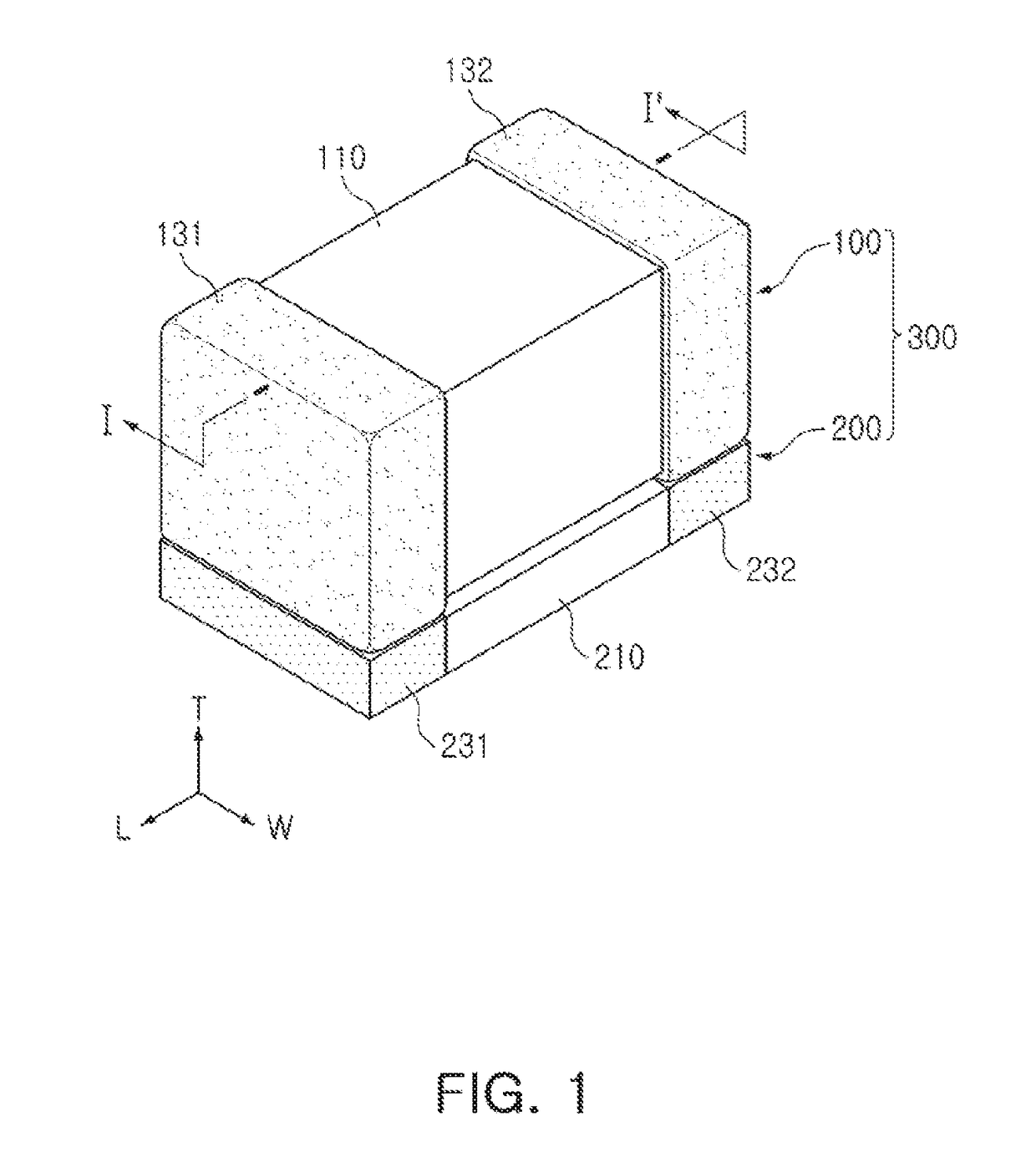
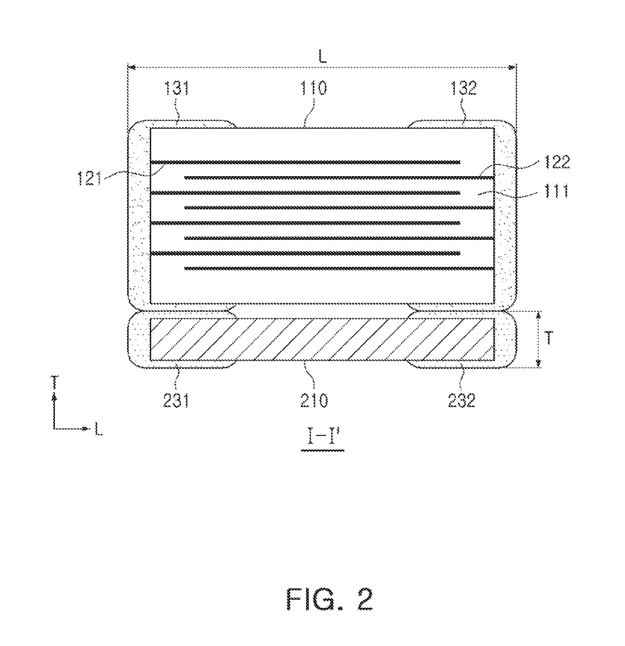
[0132]In Inventive Examples and Comparative Examples according to the present disclosure, a ceramic chip was disposed on a lower portion of a multilayer ceramic capacitor, and a composite electronic component was manufactured depending on a length of the multilayer ceramic capacitor and a mounting form of internal electrodes. Acoustic noise levels depending on a ratio (T / L) of a thickness T of a second ceramic chip 200 to a length L of the multilayer ceramic capacitor 100 was compared.

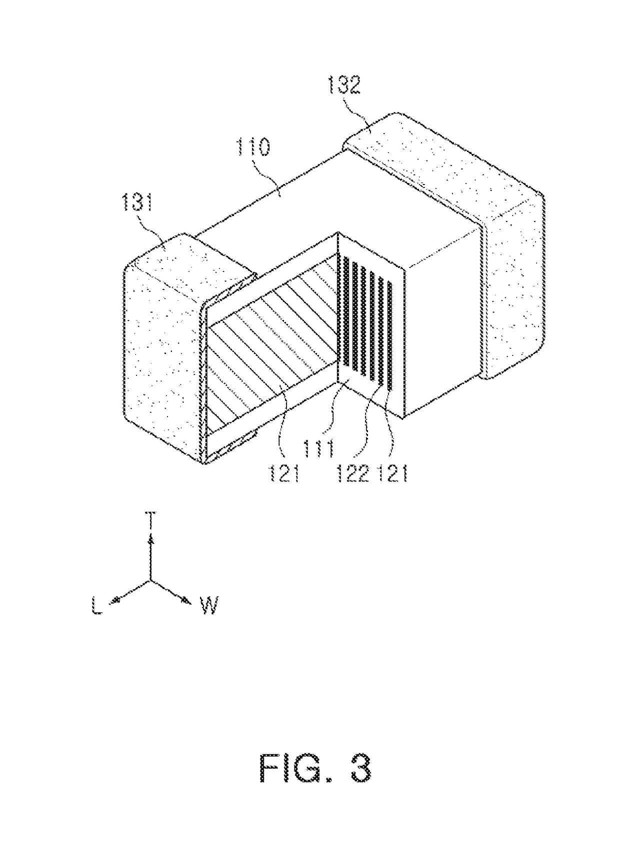
[0133]More specifically, the following [Table 1] illustrates results obtained by comparing acoustic noise levels when the length of the multilayer ceramic capacitor was 2.078 mm and the internal electrodes were stacked to be horizontal to a mounting surface of a printed circuit board.

[0134]In Comparative Examples 1 to 4 and Inventive Examples 1 to 3, each 5 samples were manufacture


PUM

PropertyMeasurementUnit
Lengthaaaaaaaaaa
Thicknessaaaaaaaaaa
Thicknessaaaaaaaaaa

Abstract

A composite electronic component includes a composite body in which a multilayer ceramic capacitor and a ceramic chip are coupled to each other, the multilayer ceramic capacitor including a first ceramic body in which a plurality of dielectric layers and internal electrodes disposed to face each other with respective dielectric layers interposed therebetween are stacked, and first and second external electrodes disposed on both end portions of the first ceramic body, and the ceramic chip being disposed on a lower portion of the multilayer ceramic capacitor and formed of a ceramic material having substantially no piezoelectric property, wherein a ratio (T/L) of thickness (T) of the ceramic chip to length (L) of the multilayer ceramic capacitor is selected to minimize vibration of the ceramic chip.

Description


Claims


Application Information

Patent Timeline
Owner SAMSUNG ELECTRO MECHANICS CO LTD
Why Eureka
Try Eureka