Low power dual-sensitivity fg-mosfet sensor for a wireless radiation dosimeter

a wireless radiation dosimeter and low-power technology, applied in the field of medical sensors, can solve the problems of high cost, high operational and cost inefficiencies, and prone to human judgment, and achieve the effect of facilitating the measurement of relatively precise, thin gate oxide layers

Active Publication Date: 2021-04-01
BEST THERATRONICS
View PDF2 Cites 0 Cited by
  • Summary
  • Abstract
  • Description
  • Claims
  • Application Information

AI Technical Summary

Benefits of technology

The technical effect of this patented method relates to improving the performance of electronic devices used during medical procedures like Xrays or fluorescence imaging (XR). By utilising small transistors made from materials called Low Power Field Effect Transistor (LPFT) chips instead of large ones, it can reduce power consumption while still maintain good signal quality even at very short distances between them. This results in improved accuracy when detecting body scans over long periods of time compared to traditional ionization techniques.

Problems solved by technology

This technical problem addressed in this patents relates to improving the quality control of radiological exposure assessments made through various imaging techniques like magnetic resonant tomography scans, especially at high levels of radiation exposures. Current systems suffer from issues including insufficient data collection capabilities, limited battery life span, difficulty in adjustment of dosages, and potential loss of image contrast caused by changes in radiation absorption properties. Additionally, existing radiosensory detectable dosemmetries lack reliabilities, making accurate monitoring important factors necessary.

Method used


Image

  • Low power dual-sensitivity fg-mosfet sensor for a wireless radiation  dosimeter
  • Low power dual-sensitivity fg-mosfet sensor for a wireless radiation  dosimeter
  • Low power dual-sensitivity fg-mosfet sensor for a wireless radiation  dosimeter

Examples


Embodiment Construction

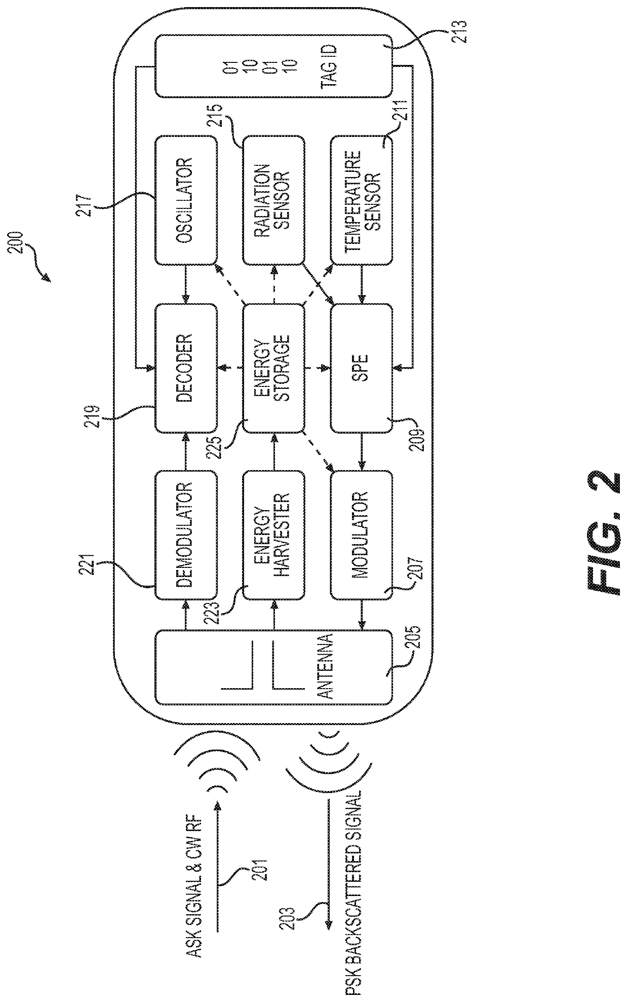
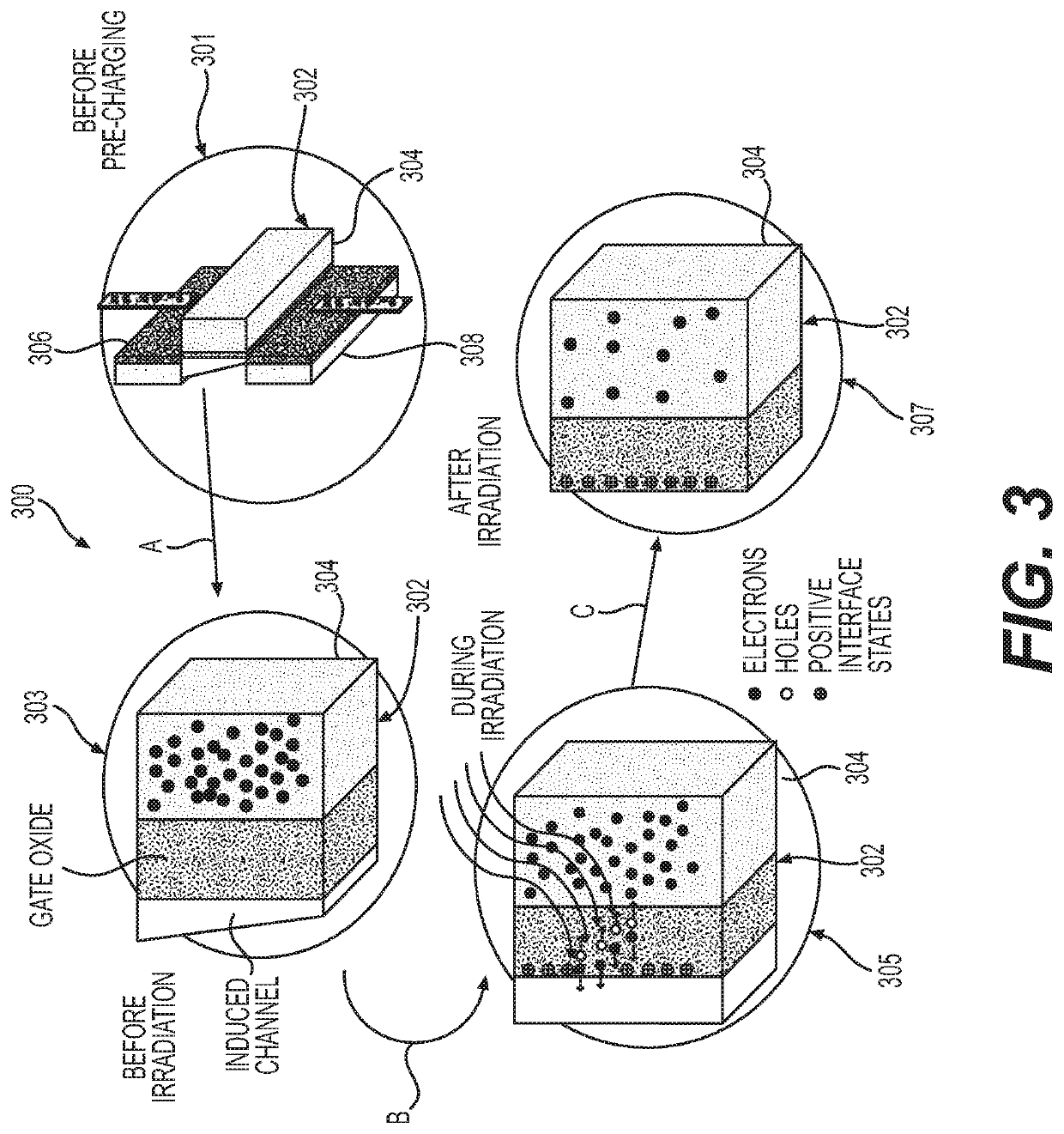
[0052]Embodiments of the disclosure relate to designs of a low-power FG-MOSFET sensor in RF-CMOS technology for use with a radio-frequency identification (RFID) wireless dosimeter chip-enabled tag, such as can be applied to blood bags, that are to be irradiated by a radiation source, such as an X-ray source, and to methods for measuring the radiation dose delivered using embodiments of a low-power FG-MOSFET sensor in RF-CMOS technology.

[0053]The term “irradiation”, as is used herein, can include, but is not limited to the conventional meaning of the term “irradiation”, i.e., exposure to high energy charge particles, e.g., electrons, protons, alpha particles, etc., or electromagnetic radiation of wave-lengths shorter than those of visible light, e.g., gamma rays, X-rays, UltraViolet, etc.

[0054]Further, as used herein, for example, the term “dosimeter” refers to a device used to measure an absorbed dose of ionizing radiation.

[0055]Also, as used herein, the term “ionizing radiation” refer


PUM


Abstract

Low-power, dual sensitivity thin oxide FG-MOSFET sensors in RF-CMOS technology for a wireless X-ray dosimeter chip, methods for radiation measurement and for charging and discharging the sensors are described. The FG-MOSFET sensor from a 0.13 μm (RF-CMOS process, includes a thin oxide layer having a device region, a source and a drain associated with the device well region, separated by a channel region, a floating gate extending over the channel region, and a floating gate extension extending over the thin oxide layer adjacent to the device well region. In a matched sensor pair for dual sensitivity radiation measurement, the floating gate and the floating gate extension of a FG-MOSFET higher sensitivity sensor are without a salicide layer or a silicide layer formed thereon and the floating gate and the floating gate extension of a FG-MOSFET lower sensitivity sensor have a salicide layer or a silicide layer formed thereon.

Description


Claims


Application Information

Patent Timeline
Owner BEST THERATRONICS
Why Eureka
Try Eureka