Semiconductor memory device

Active Publication Date: 2006-07-11
KIOXIA CORP
View PDF14 Cites 36 Cited by
  • Summary
  • Abstract
  • Description
  • Claims
  • Application Information

AI Technical Summary

Benefits of technology

[0026]According to an aspect of the invention, a semiconductor memory device comprises a plurality of memory cell areas, each of which includes a plurality of memory cells arrayed in a matrix and has a data I/O portion; a plurality of buffers, each of which is coupled to the data I/O portion at each memory cell area to temporarily store data to be written into the memory cell area and data read out from the memory cell area; a plurality of I/O terminals, each of which is configured to receive external data to be written into the memory cell area and externally read out from the memory; and an error correction circuit located between the plurality of I/O terminals and the plurality of buffers, the error correction circuit includes a coder configured to generate check bits for error correcting and to append the check bits to the data to be written into the memory cell area and a decoder configured for error correcting the data read out from the memory cell area with the generated check bits, the error correction circuit operates to allocate a set of check bits to an information unit of M×N bits (N denotes an integer of two or more) to execute at least one process of coding and decoding by parallel processing N-bit data, where M denotes the number of bits in a unit of data to be written into and read out from each memory cell area.

Problems solved by technology

The NAND-type flash memory is known to deteriorate its cell property through repeated operations of rewriting, and to vary data after it is left for a long time.
The 8 or 16-time computation during the one input cycle needs a fast operation, which can not be achieved practically because a special process is required, for example.

Method used


Image

  • Semiconductor memory device
  • Semiconductor memory device
  • Semiconductor memory device

Examples


Example

(1) First Embodiment

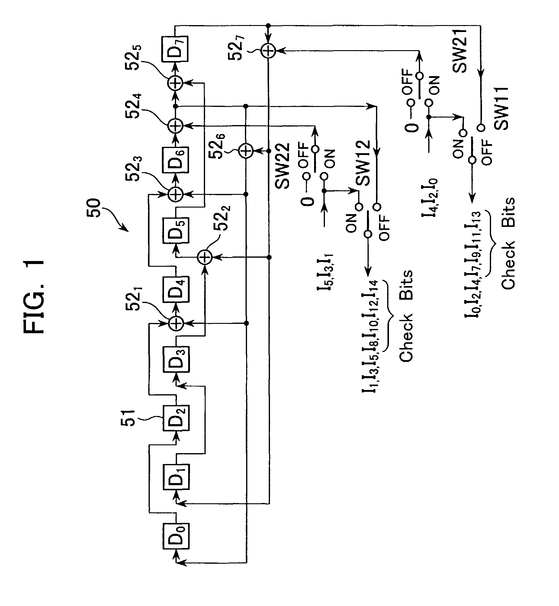
[0055]In order to provide an understanding of the present invention, 2-bit error correction is exemplified as a first embodiment with the number of information bits, k=7, a code length, n=15, and the number of correction bits, t=2.

(1-1) Coder

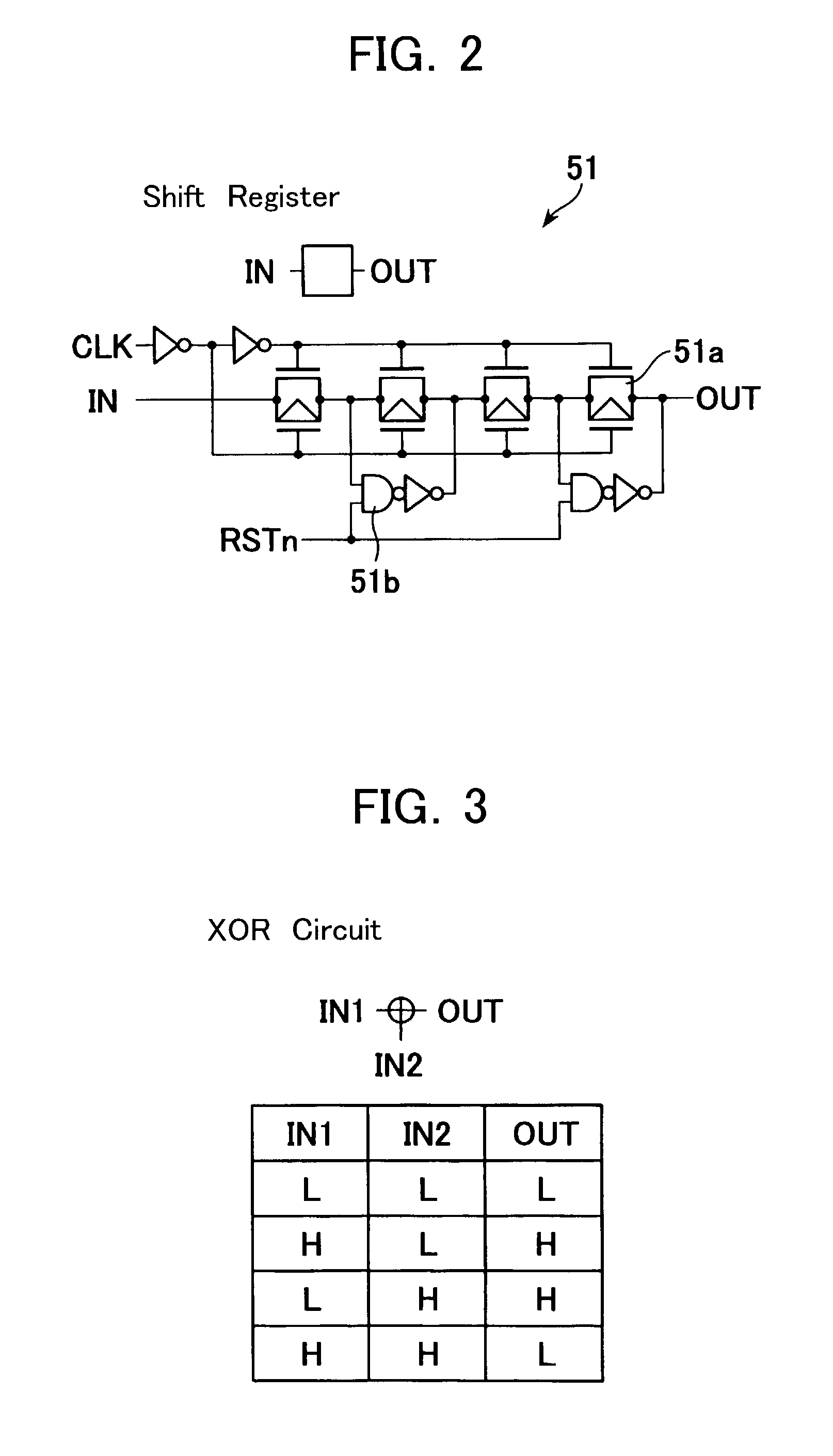
[0056]When input data I0 enters the conventional coder 11 shown in FIG. 22, the input data I0 is added at the XOR circuit 124 to the term of X7 in the coder, then multiplied by X. Each register 11 in the coder 10 in the initial state has a value of 0, which is referred to as (0). Accordingly:

(0+I0X7)X   (17)

When next input data I1 enters the coder 10, the input data I1 is added to the term of X7 in the coder 10, then multiplied by X to yield:

((0+I0X7)X+I1X7)X   (18)

[0057]When next input data I2 enters the coder 10, the input data I2 is added to the term of X7 in the coder 10, then multiplied by X to yield:

(((0+I0X7)X+I1X7)X+I2X7)X   (19)

[0058]Similarly, after input data, up to I6, enters the coder 10, the following is given:

((((

Example

(2) Second Embodiment

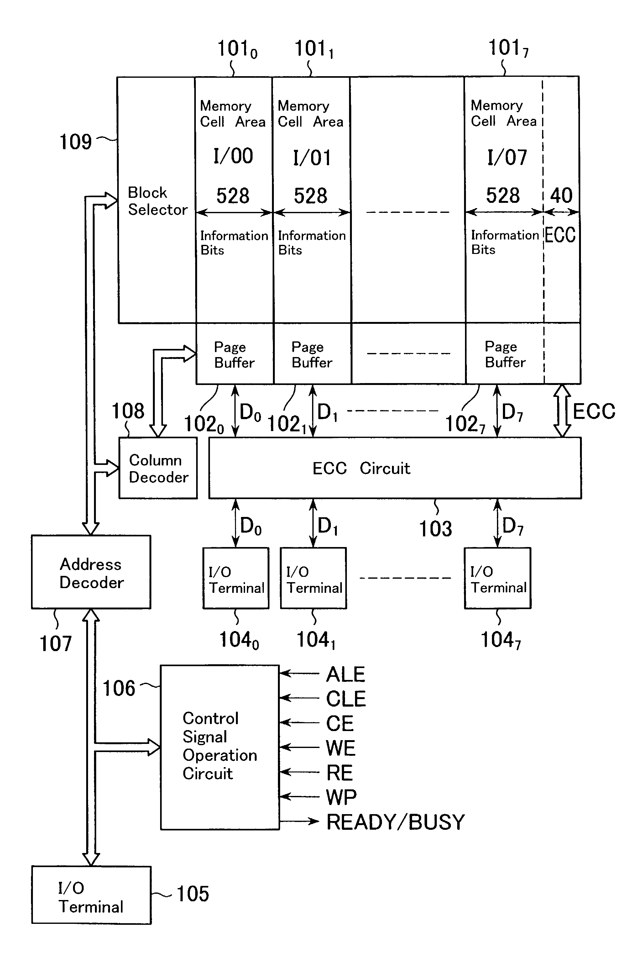
[0084]FIG. 7 is a block diagram showing a NAND-type flash memory according to a second embodiment, which mounts an ECC circuit on a chip.

[0085]The memory comprises eight memory cell areas 1010, 1011, 1012, . . . , 1017. Eight page buffers 1020, 1021, 1022, . . . , 1027 are provided corresponding to the memory cell areas 1010, 1011, 1012, . . . , 1017 to temporarily store data to be written in and read out of the memory cell areas 1010, 1011, 1012, . . . , 1017. Between the page buffers 1020–1027 and I / 0 terminals 1040, 1041, . . . , 1047, an ECC circuit 103 is provided to generate check bits, ECC, for correcting errors in the write data and to correct errors in the read data using the check bits (ECC). Different from the conventional type, for error detection and correction, the ECC circuit 103 adds 40 check bits commonly to information bits consisting of 528 bits ×8 I / O=4224 bits data (M=528, N=8) that can be read out of and written into all memory cell areas


PUM


Abstract

An ECC circuit (103) is located between I/O terminals (1040–1047) and page buffers (1020–1027). The ECC circuit (103) includes a coder configured to generate check bits (ECC) for error correcting and attach the check bits to data to be written into a plurality of memory cell areas (1010–1017), and a decoder configured to employ the generated check bits (ECC) for error correcting the data read out from the memory cell areas (1010–1017). The ECC circuit (103) allocates a set of 40 check bits (ECC) to an information bit length of 4224=(528×8) bits to execute coding and decoding by parallel processing 8-bit data, where data of 528 bits is defined as a unit to be written into and read out from one memory cell area (101j).

Description


Claims


Application Information

Patent Timeline
Owner KIOXIA CORP
Why Eureka
Try Eureka