Gallium nitride-base infrared visable wavelength conversion detector

An infrared detector and wavelength conversion technology, applied in semiconductor devices, electrical components, circuits, etc., can solve problems such as unreliability, expensive integrated systems, thermal shock effects, etc., and achieve the effect of reducing technical difficulty and cost, and simplifying the system structure

Inactive Publication Date: 2008-10-08
SHANGHAI INST OF TECHNICAL PHYSICS - CHINESE ACAD OF SCI +1
View PDF3 Cites 0 Cited by
  • Summary
  • Abstract
  • Description
  • Claims
  • Application Information

AI Technical Summary

Benefits of technology

This patented technology allows for better control over how much electrical current flows through an optically thin film called a multiquantum well (MQW) formed on top of another semiconductor crystal called gallium nitride monocrystals (gallium arsenide), created from indium phosphate (InP)). These MQW layers help absorb visible lights while transmitting them efficiently at longer wave lengths like red waves. Additionally, this method simplifies the manufacturing processes compared to existing methods such as cathodolayers and lamps without requiring any specialized components. Overall, these techniques improve efficiency and performance of optoelectronic systems.

Problems solved by technology

Technological Problem: Current methods used for converting infra red signals (IR) onto different types of electronic components require multiple layers or wires that connect them together at specific points along their length. These connections increase complexity and costs associated therewith. Additionally, current IR detection techniques may be affected when subjected to temperature changes due to heat generated during operation.

Method used


Image

  • Gallium nitride-base infrared visable wavelength conversion detector
  • Gallium nitride-base infrared visable wavelength conversion detector

Examples


Embodiment Construction

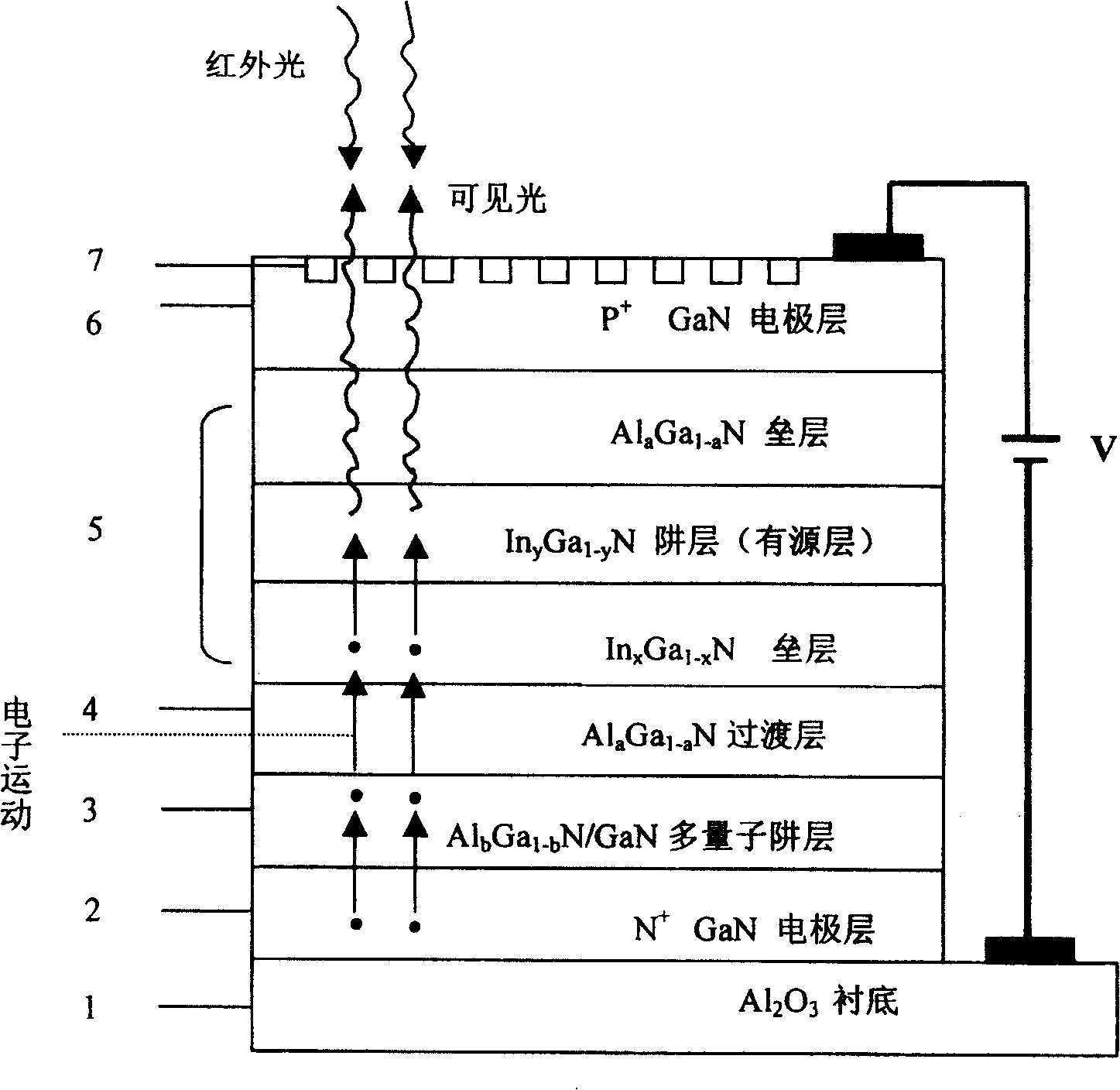
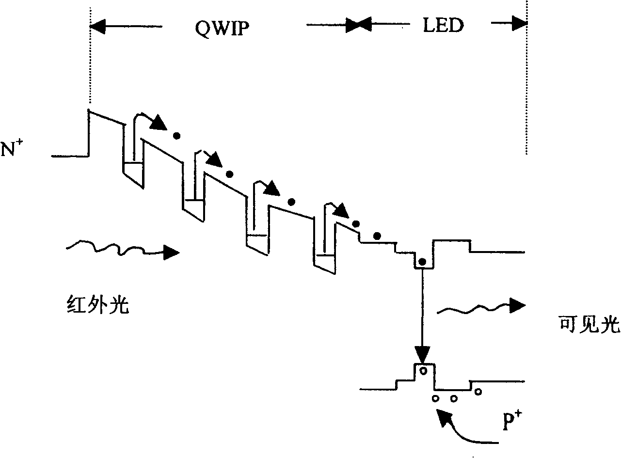
[0017] The following is an example of an infrared-visible wavelength conversion detector coupled in series with an N-type QWIP and a green LED, wherein the infrared absorption peak of the N-type QWIP is set at around 2.9 microns, and the peak wavelength of the EL spectrum of the LED is at 525nm. The figure further elaborates the specific embodiment of the present invention:

[0018] The detector of the present invention is a typical technology utilizing semiconductor material epitaxy, such as molecular beam epitaxy technology, metal organic chemical vapor deposition technology, etc., in Al 2 o 3 Sequential growth on the sapphire substrate 1:

[0019] n*-GaN lower electrode layer 2;

[0020] Alternate growth of 50 cycles of 10nm thick Al 0.35 Ga 0.65 N barrier layer (51 layers) and 3.5nm thick GaN potential well layer (50 layers), wherein the doping concentration in the GaN quantum well is 8*10 17 cm -3 , thereby forming an infrared detector 3 with multiple quantum wells;


PUM


Abstract

An infrared - visible wavelength converting detector with gallium nitride base is prepared by gallium nitride based material and series - couples multiple quantum well infrared detector as well as luminous diode on the same chip. It features that multiple quantum well infrared detector is used to convert infrared radiation signal to be infrared photoelectric signal and then luminous diode is used to infrared photoelectric signal to be light signal of visible waveband.

Description


Claims


Application Information

Patent Timeline
Owner SHANGHAI INST OF TECHNICAL PHYSICS - CHINESE ACAD OF SCI
Why Eureka
Try Eureka