Deep ultraviolet epitaxial wafer and preparation method thereof
An epitaxial wafer, deep ultraviolet technology, applied in electrical components, circuits, semiconductor devices, etc., can solve the problems of serious absorption of deep ultraviolet light by P-type GaN, low luminous efficiency of deep ultraviolet LEDs, and inability to achieve high Al doping, etc. Achieve the effect of improving injection, realizing ohmic contact, and improving luminous efficiency
- Summary
- Abstract
- Description
- Claims
- Application Information
AI Technical Summary
Benefits of technology
Problems solved by technology
Method used
Image

Examples
preparation example Construction
[0028] The embodiment of the present invention provides a method for preparing a deep ultraviolet epitaxial wafer, comprising the steps of:
[0029] An aluminum nitride thin film buffer layer, a U-type aluminum gallium nitride layer, an N-type aluminum gallium nitride layer, a quantum well layer and a P-type gallium nitride layer are sequentially grown on the substrate, and the P-type gallium nitride includes sequentially grown P type aluminum gallium nitride layer, aluminum nitride layer, p-doped gallium nitride layer and heavily doped p-type aluminum gallium nitride layer.
[0030] It can be seen from the above description that the deep ultraviolet epitaxial wafer includes P-type GaN, and P-type GaN includes a P-type AlGaN layer, an AlN layer, a P-doped GaN layer, and a heavily doped P-type GaN layer. AlGaN layer. Among them, the P-type AlGaN layer can effectively reduce the absorption of deep ultraviolet light; on the basis of effectively reducing the absorption of deep ultra
Embodiment 1
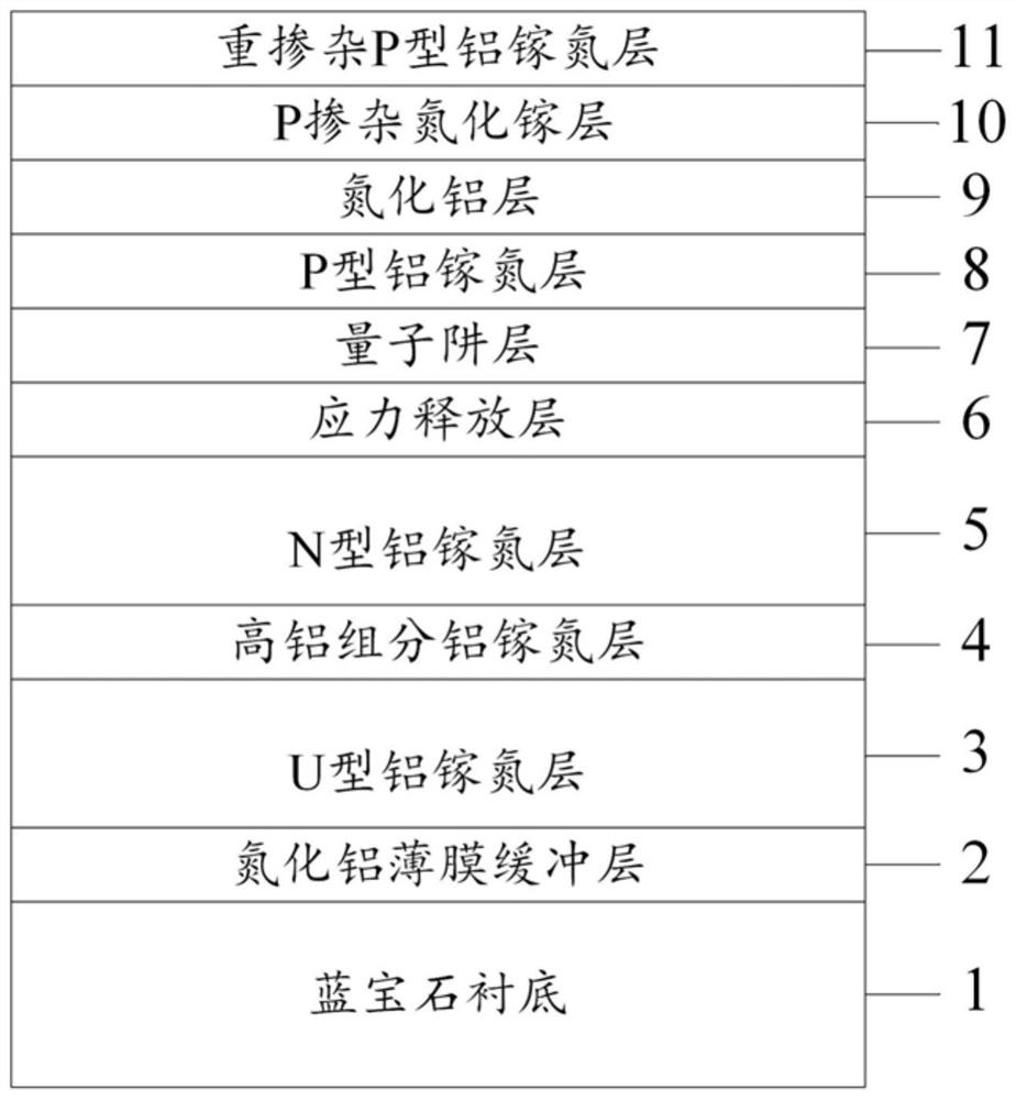
[0045] Please refer to figure 1 , a deep ultraviolet epitaxial wafer, including an aluminum nitride film buffer layer, a U-type aluminum-gallium-nitride layer, an N-type aluminum-gallium-nitride layer, a quantum well layer and a P-type gallium nitride layer grown sequentially on a substrate.
[0046] P-type gallium nitride (GaN) includes a P-type aluminum gallium nitride (AlGaN) layer, an aluminum nitride (AlN) layer, a P-doped gallium nitride layer and a heavily doped P-type aluminum gallium nitride layer grown sequentially.
[0047] Specifically, the deep ultraviolet epitaxial wafer includes an AlN film buffer layer with a thickness of 15-20nm, a U-shaped AlGaN layer with a thickness of 1.5-2.5um, and a high Al composition AlGaN layer with a thickness of 25-35nm grown on the substrate in sequence. , an N-type AlGaN layer with a thickness of 1.5-2.5um, a stress release layer (gallium nitride) with a thickness of 70-90nm, an active region (quantum well layer) and a P-type GaN lay
Embodiment 2
[0051] A method for preparing a deep ultraviolet epitaxial wafer, comprising the steps of:
[0052] An aluminum nitride thin film buffer layer, a U-type aluminum gallium nitride layer, an N-type aluminum gallium nitride layer, a quantum well layer and a P-type gallium nitride layer are sequentially grown on the substrate, and the P-type gallium nitride includes sequentially grown P type aluminum gallium nitride layer, aluminum nitride layer, p-doped gallium nitride layer and heavily doped p-type aluminum gallium nitride layer.
[0053] Specifically, S1. Sputter an AlN thin film buffer layer with a thickness of 20 nm on the (0001) plane sapphire substrate layer (non-PSS) by means of magnetron sputtering.
[0054] S2, growing a 2um U-shaped AlGaN layer on the AlN film buffer layer.
[0055] S3, growing a 30nm-thick heavy Al component AlGaN layer and growing a 1.9um N-type AlGaN layer sequentially on the U-type AlGaN layer.
[0056] S4. An 80nm stress release layer (gallium nitrid
PUM
| Property | Measurement | Unit |
|---|---|---|
| Thickness | aaaaa | aaaaa |
| Thickness | aaaaa | aaaaa |
| Thickness | aaaaa | aaaaa |
Abstract
Description
Claims
Application Information
 - R&D Engineer
- R&D Manager
- IP Professional
- Industry Leading Data Capabilities
- Powerful AI technology
- Patent DNA Extraction
Browse by: Latest US Patents, China's latest patents, Technical Efficacy Thesaurus, Application Domain, Technology Topic.
© 2024 PatSnap. All rights reserved.Legal|Privacy policy|Modern Slavery Act Transparency Statement|Sitemap