A porous active layer field effect ultraviolet detector and a preparation method thereof
A technology of ultraviolet detector and active layer, which is applied in the field of ultraviolet detection, can solve the problems affecting the sensitivity of ultraviolet light detection, etc., and achieve the effect of simple structure, broad application prospect and wide frequency band
- Summary
- Abstract
- Description
- Claims
- Application Information
AI Technical Summary
Problems solved by technology
Method used
Image

Examples
Example Embodiment
[0029] Example 1
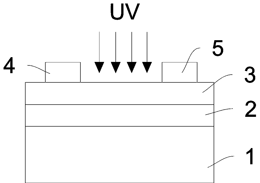
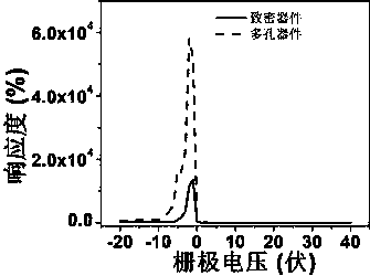
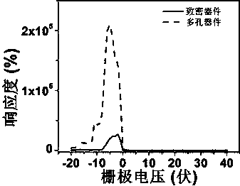
[0030] Such as figure 1 Shown, a porous active layer field effect ultraviolet detector, including SiO 2 / Si substrate, porous active layer 3, source electrode 4 and drain electrode 5, the SiO 2 / Si substrate includes Si layer below and SiO above 2 Layer, the Si layer is the gate electrode 1, SiO 2 The layer is an insulating layer 2, and the porous active layer 3 is arranged on SiO 2 On the / Si substrate, the porous active layer 3 is obtained by preparing the active layer on the microsphere template and removing the microspheres. The material of the active layer is metal oxide semiconductor ZnO, IZO, TiO 2 , IGZO or SnO 2 , IZO is used in this embodiment. The active layer material uses a metal oxide semiconductor that is sensitive to ultraviolet light; the porous active layer structure can make ultraviolet light directly act on the interface between the active layer and the insulating layer, reducing the absorption of ultraviolet light by the active layer film
Example Embodiment
[0032] Example 2
[0033] This embodiment is basically the same as Embodiment 1, and the similarities will not be repeated. The difference is that the porous active layer 3 is obtained by preparing an active layer on a porous template. The source electrode 4 and the drain electrode 5 are made of Ni.
Example Embodiment
[0034] Example 3
[0035] The preparation of a porous active layer field-effect ultraviolet detector includes the following steps:
[0036] Step 1: Choose SiO 2 / Si substrate, where Si layer is used as gate electrode, SiO 2 The layer is an insulating layer; before use, the SiO 2 / Si substrate is placed in ultrasonic, and washed with acetone, absolute ethanol and deionized water for 15 minutes to remove SiO 2 / The contaminants on the Si substrate are then blown dry with nitrogen.
[0037] Step 2: In SiO 2 / Si substrate prepared polystyrene (PS) microsphere template. The specific method is: preparing an aqueous solution of PS microspheres with a mass percentage concentration of 2%, stirring magnetically for 1 hour at room temperature, and then ultrasonically dispersing for 20 minutes, and the diameter of the PS microspheres is 500 nm. Drop PS microsphere aqueous solution on SiO 2 / Si substrate, then vacuum freeze-drying, when the moisture is completely removed, the PS microsphe
PUM
| Property | Measurement | Unit |
|---|---|---|
| Aperture | aaaaa | aaaaa |
| Thickness | aaaaa | aaaaa |
| Thickness | aaaaa | aaaaa |
Abstract
Description
Claims
Application Information
 - R&D Engineer
- R&D Manager
- IP Professional
- Industry Leading Data Capabilities
- Powerful AI technology
- Patent DNA Extraction
Browse by: Latest US Patents, China's latest patents, Technical Efficacy Thesaurus, Application Domain, Technology Topic.
© 2024 PatSnap. All rights reserved.Legal|Privacy policy|Modern Slavery Act Transparency Statement|Sitemap