Solid-state imaging device, method for producing same, and camera
A solid-state imaging device and control gate technology, which is applied in the field of cameras, can solve the problems of reducing the reading ability of transfer gates, etc.
- Summary
- Abstract
- Description
- Claims
- Application Information
AI Technical Summary
Problems solved by technology
Method used
Image

Examples
no. 2 example
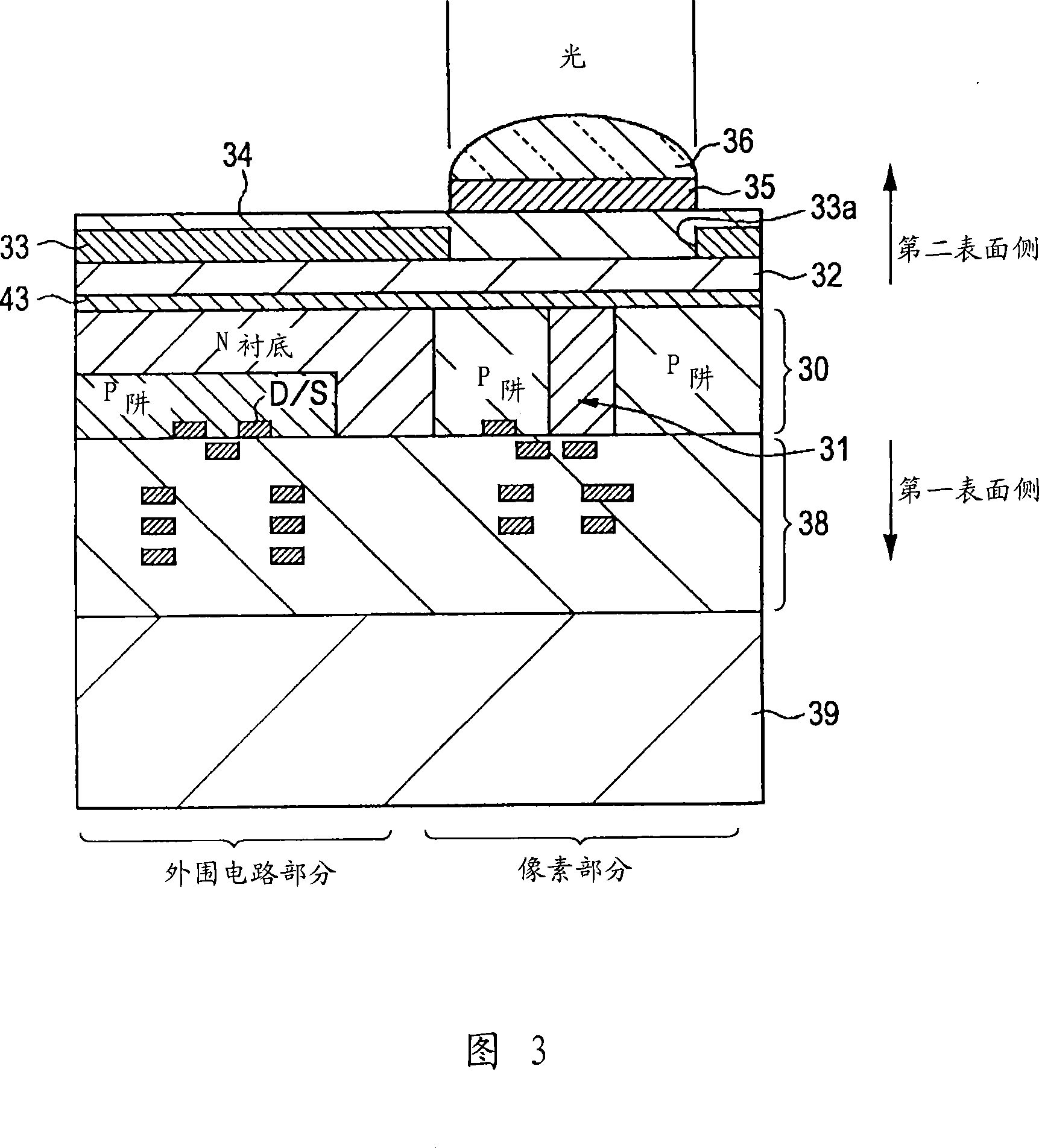
[0117] 11 is a partial sectional view of a pixel portion of a substrate 30 of a solid-state imaging device according to the second embodiment. The same elements as those in the first embodiment are denoted by the same reference numerals, and redundant descriptions will not be repeated.
[0118]Two control gates, namely, a first control gate 52-1 and a second control gate 52-2 are formed on the first surface of the substrate 30 with a gate insulating film (not shown) interposed therebetween. The first control gate 52-1 is located between the transfer gate 51 and the second control gate 52-2. The first and second control gates 52 - 1 and 52 - 2 are superimposed on the photodetector 31 . The first and second control gates 52-1 and 52-2 are made of, for example, polysilicon. Each of the first and second control gates 52 - 1 and 52 - 2 preferably has a thickness comparable to that of the transfer gate 51 in consideration of workability and resistance. Light is incident on the secon
no. 3 example
[0133] 13 is a partial cross-sectional view of a pixel portion of a substrate 30 of a solid-state imaging device according to the third embodiment. The same elements as those in the first embodiment are denoted by the same reference numerals, and redundant descriptions will not be repeated.
[0134] The control gate 52 is formed on the first surface of the substrate 30 with a gate insulating film (not shown) interposed therebetween. In this embodiment, control gate 52 partially overlaps photodetector 31 . The hole accumulation region 44 is not formed under the control gate 52 . That is, a region where only the control gate 52 is located and a region where only the hole accumulation region 44 is located next to the transfer gate 51 are formed. Alternatively, the hole accumulation region 44 may be formed on the entire surface of the photodetector 31 . In addition, the control gate 52 and the hole accumulation region 44 may be reversely arranged.
[0135] The solid-state imaging
no. 4 example
[0148] 14 is a partial sectional view of a pixel portion of a solid-state imaging device according to a fourth embodiment. The same elements as those in the first embodiment are denoted by the same reference numerals, and redundant descriptions will not be repeated.
[0149] The solid-state imaging device according to this embodiment includes a transparent conductive film 74 on the light-receiving surface of the photodetector 31 constituting a photodiode as a photoelectric converter, that is, in the region of the first conductivity type (n-type charge accumulation region) 41 On the light-receiving surface of , a single-layer insulating film 71 is provided therebetween. The solid-state imaging device is configured in such a manner that a negative voltage is applied to the transparent conductive film 74 . The transparent conductive film 74 functions as a control gate, which controls the potential of the light receiving surface. The transparent conductive film 74 is covered with a
PUM
| Property | Measurement | Unit |
|---|---|---|
| Thickness | aaaaa | aaaaa |
| Thickness | aaaaa | aaaaa |
| Thickness | aaaaa | aaaaa |
Abstract
Description
Claims
Application Information
 - R&D Engineer
- R&D Manager
- IP Professional
- Industry Leading Data Capabilities
- Powerful AI technology
- Patent DNA Extraction
Browse by: Latest US Patents, China's latest patents, Technical Efficacy Thesaurus, Application Domain, Technology Topic.
© 2024 PatSnap. All rights reserved.Legal|Privacy policy|Modern Slavery Act Transparency Statement|Sitemap