Method for preventing abnormal chip etching caused by damage to parts

A wafer and etching technology, used in semiconductor/solid-state device manufacturing, electrical components, circuits, etc., to reduce the chance of unqualified products

Inactive Publication Date: 2010-06-09
HEJIAN TECH SUZHOU
View PDF0 Cites 1 Cited by
  • Summary
  • Abstract
  • Description
  • Claims
  • Application Information

AI Technical Summary

Benefits of technology

The technical effect of this technology allows for accurate identification or detection of any problems with certain parts within machines' radios without stopping them down completely until they are fixed out again after being repaired during maintenance work on their own equipment.

Problems solved by technology

In this technical problem addressed in this patents relates to improving the accuracy and reliability of detecting changes caused during processing steps such as dry or liquid etches on substrate materials like silicone rubber (SR) without causing damage or scrapings.

Method used


Image

  • Method for preventing abnormal chip etching caused by damage to parts
  • Method for preventing abnormal chip etching caused by damage to parts

Examples


Embodiment Construction

[0018] A method for preventing abnormal wafer etching caused by damage to parts according to the present invention will be further described in detail below in conjunction with specific embodiments.

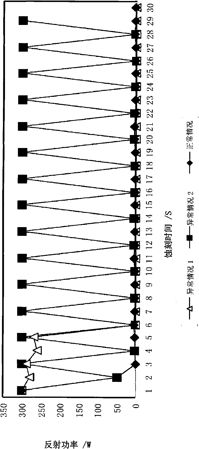
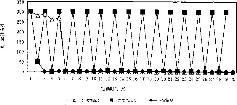
[0019] One embodiment of the method of the present invention is a method for preventing the wafer from being scrapped due to abnormal radio frequency reflection power, such as figure 1 , where the rhombus line represents the change of reflected power with the increase of etching time under normal conditions; the upper triangle line and square line represent the change of reflected power with the increase of etching time under abnormal conditions 1 and 2, respectively The changing situation will be described below with regard to abnormal situation 1 and abnormal situation 2.

[0020] In this embodiment, first, the wafer to be dry-etched is placed on the machine, and a predetermined time period and a predetermined standard have been set in the machine, and the specific value of the pr


PUM


Abstract

The invention relates to a method for preventing abnormal chip etching caused by damage to parts. The method comprises the following steps of: placing the chip to be etched on a dry type etching machine station, wherein a preset time segment and a preset standard are set in the machine station; and comparing values of measured parameters with the preset standard in the whole process of the dry type etching of the chip, and if the average value of the measured parameters during the preset time segment is higher than the preset standard, automatically stopping the dry type etching process by the machine station. By adopting the method, the abnormity of a radio frequency generator of the machine station can be known in time, so that the probability of generating unqualified products is reduced.

Description


Claims


Application Information

Patent Timeline
Owner HEJIAN TECH SUZHOU
Why Eureka
Try Eureka