Manufacturing method of surface mounted device resistor

A manufacturing method and technology of chip resistors, applied in resistor manufacturing, resistors, resistors with terminals, etc., can solve the problems of weakened market competitiveness, high production costs, thick thickness, etc., to enhance market competitiveness and ensure The effect of on-connectivity and production cost reduction

Active Publication Date: 2011-06-01
UNIROYAL ELECTRONICS IND
View PDF0 Cites 8 Cited by
  • Summary
  • Abstract
  • Description
  • Claims
  • Application Information

AI Technical Summary

Benefits of technology

This technology allows for better control over how much electrical current flows through an electronic device's components during operation compared to traditional methods like solder or wires used for connecting circuitry together. It achieves this by depositing layers containing metal powders onto surfaces where they will actively participate in electric conduction processes. By doing these techniques, the manufacturing costs associated with producing such devices may decrease while maintain their quality level comparable to those produced from pure metals.

Problems solved by technology

This patented technical problem addressed in this patents relates to improving the accuracy and consistency during chips' manufacture due to variations caused from factors like surface roughness or bending stress that can affect how well the resistance values change when they hit certain points inside the circuit board. Additionally, current methods for forming these layers require expensive materials such as Silver Paddle material and solder powders which increase costs compared to simpler processes.

Method used


Image

  • Manufacturing method of surface mounted device resistor
  • Manufacturing method of surface mounted device resistor
  • Manufacturing method of surface mounted device resistor

Examples


Embodiment

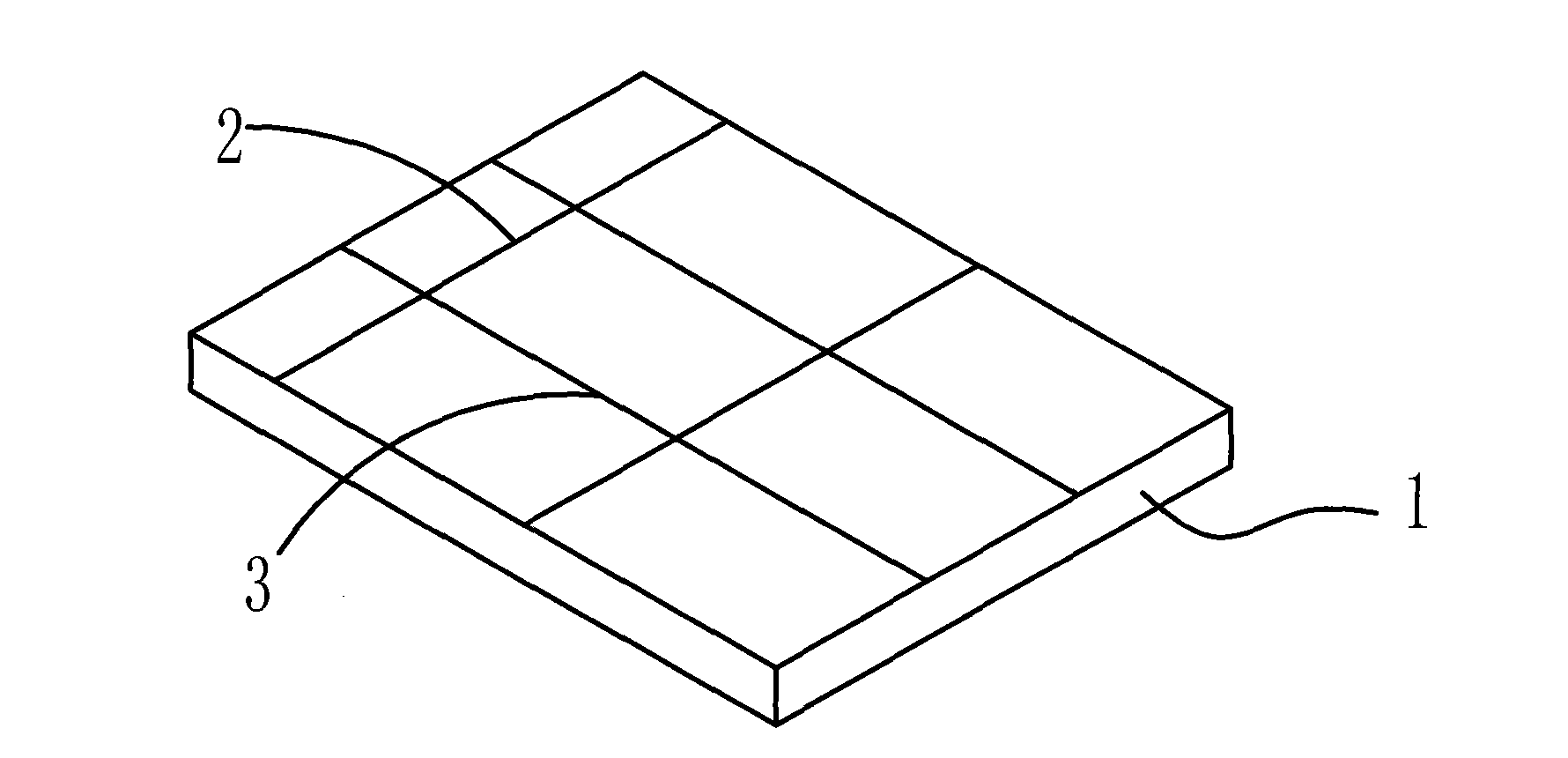
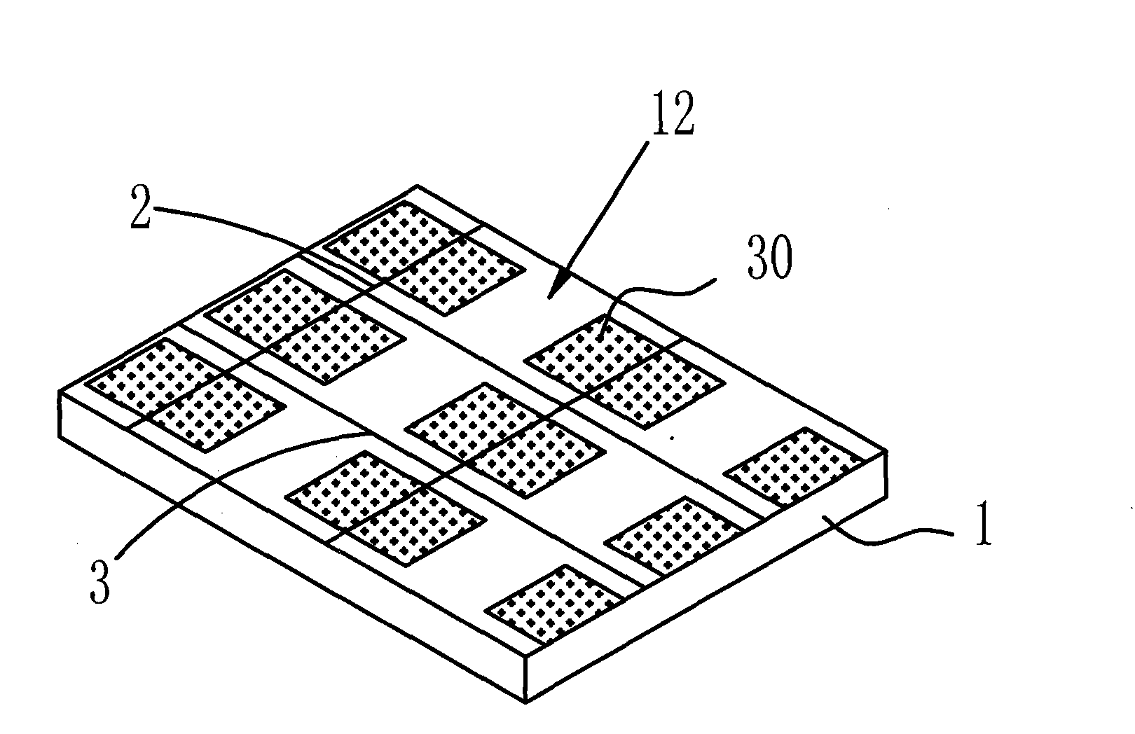
[0052] Embodiment: A kind of manufacturing method of chip resistor, is based on using direction, and its manufacturing steps are as follows:

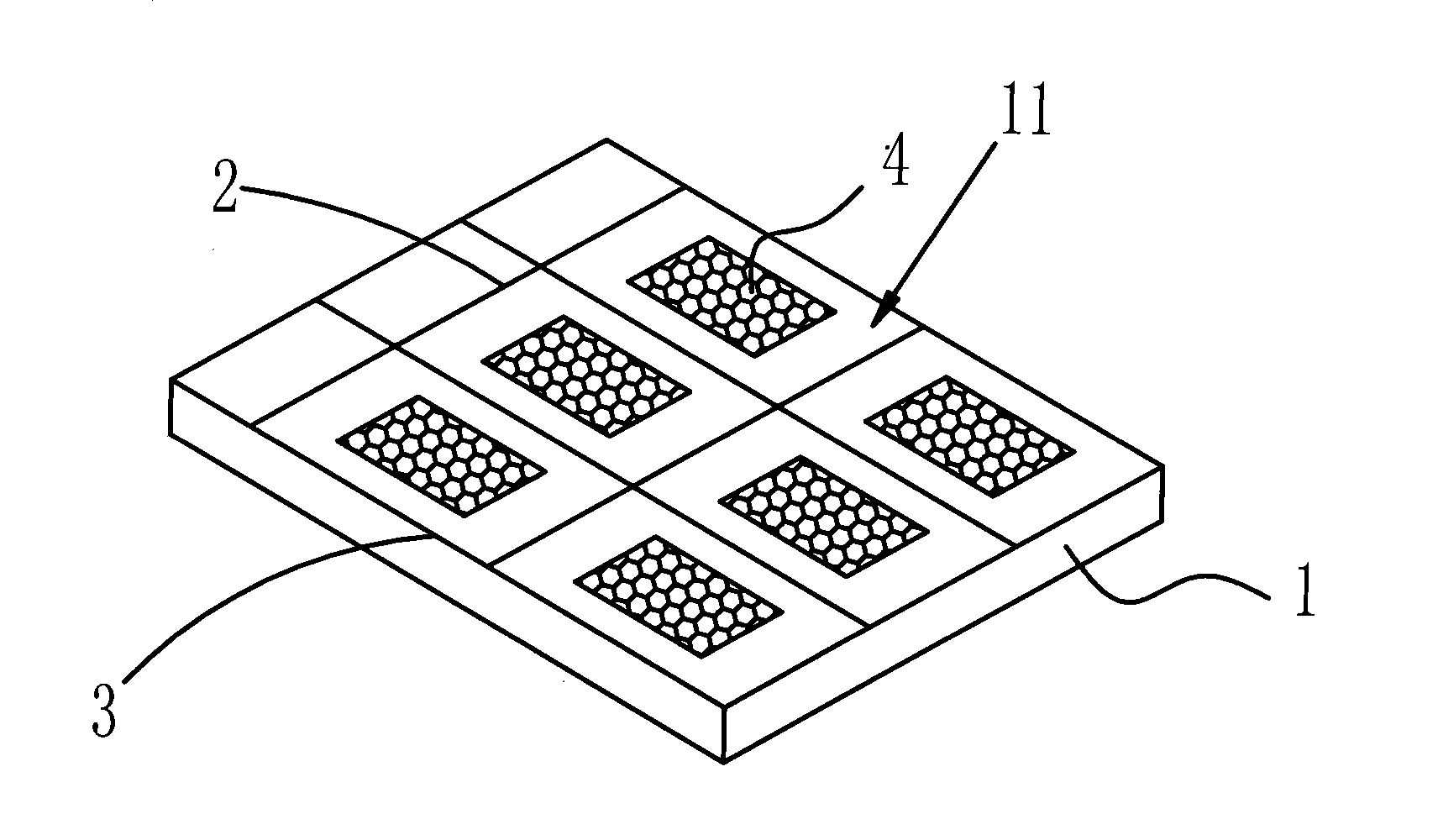
[0053] a. Prepare an insulating substrate 1, and form a plurality of horizontal folding lines 2 and a plurality of longitudinal folding lines 3 on the upper surface 11 and the lower surface 12 of the insulating substrate evenly corresponding to the grid;

[0054] b. Print the silver paste on the lower surface 12 of the insulating substrate 1 at set intervals by screen printing, dry and sinter to form each back electrode 30, and the position of each back electrode 30 is to correspond to the horizontal fold The line 2 is the transverse center line and each back electrode 30 is located in the middle of two adjacent longitudinal folding lines 3;

[0055] c. Print the resistance paste on the upper surface 11 of the insulating substrate 1 by screen printing, dry and sinter to form each resistance layer 4, and the position of each resistance laye


PUM


Abstract

The invention discloses a manufacturing method of a surface mounted device (SMD) resistor. The method for manufacturing a positive electrode of the SMD resistor comprises the following steps: firstly, printing a resistive layer; secondly, printing and covering a positive auxiliary electrode at both sides of a position in which the resistive layer is close to the positive electrode; and thirdly, sputtering to form the positive electrode, thus ensuring the connectivity between the positive electrode and the resistive layer and strengthening the stability of a product. The positive electrode is used for sputtering a conductive material which takes silver as a main composition in a vacuum sputtering mode. The sputtered conductive material can be sputtered uniformly to a substrate surface. A sputtered electrode layer has the advantages of thin film and excellent uniformity, thus ensuring the uniformity of the film thickness of the positive electrode and overcoming the shortcoming that the initial value of the resistor is easy-dispersed. Besides, the cost of the conductive material taking the silver as the main component is lower than that of silver paste, and the amount of the conductive materials is less, thus effectively reducing the production cost of products, improving the market competitiveness of the products and being suitable for batch production.

Description


Claims


Application Information

Patent Timeline
Owner UNIROYAL ELECTRONICS IND
Why Eureka
Try Eureka