Intermediate reflection structure in thin film solar cells

A solar cell and thin film technology, applied in circuits, photovoltaic power generation, electrical components, etc., can solve problems such as being unsuitable and not conducive to good contact of devices, and achieve the effects of easy production, good electrical contact, and good adhesion

Inactive Publication Date: 2014-09-03
TEL太阳能公司
View PDF1 Cites 2 Cited by
  • Summary
  • Abstract
  • Description
  • Claims
  • Application Information

AI Technical Summary

Benefits of technology

This patented technology allows for efficient production of multiple junctions (or multijunction) solar cells with improved performance compared to traditional single junction devices. By implementing both active regions on different materials together instead of just two separately, these techniques lead to higher efficiency than current methods while also improving their overall effectiveness over time due to better bonding or electric connection among them.

Problems solved by technology

This patented technical problem addressed in the patant relates to improving the performance characteristics of certain electronic components that require efficient reflection of incident sunlight onto their corresponding surfaces during power generation. Specifically, there has been proposed various techniques involving depositing different materials over each component's surface beforehand, but these approaches have limitations due to factors including material quality, process conditions, and impurities introduced through previous steps.

Method used


Image

  • Intermediate reflection structure in thin film solar cells
  • Intermediate reflection structure in thin film solar cells
  • Intermediate reflection structure in thin film solar cells

Examples


Embodiment Construction

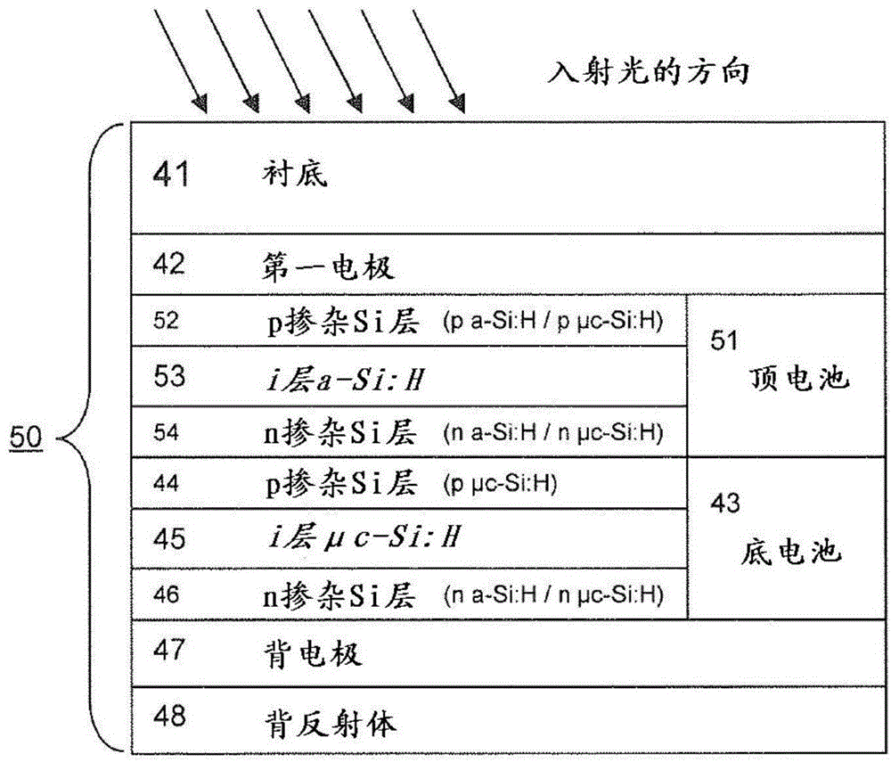
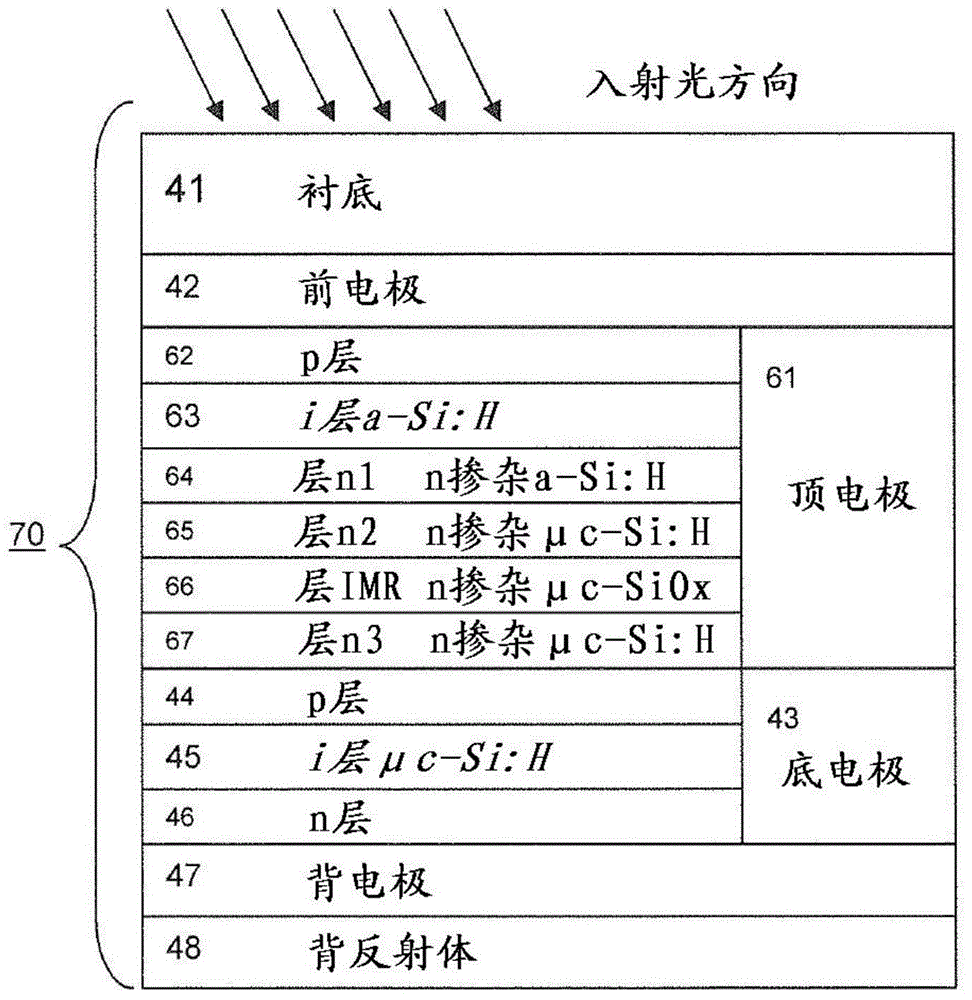
[0082] The focus of the present invention is as image 3 The design and characteristics of the n-layer of the amorphous top cell 61 of the amorphous micromorph tandem cell 70 are depicted. However, it can be applied to any thin film silicon multi-junction cell of this type. The amorphous top cell here means the first cell on the light incident side characterized by an amorphous i-layer 63 (which may also be graded or multiple i-layers as long as it is amorphous).

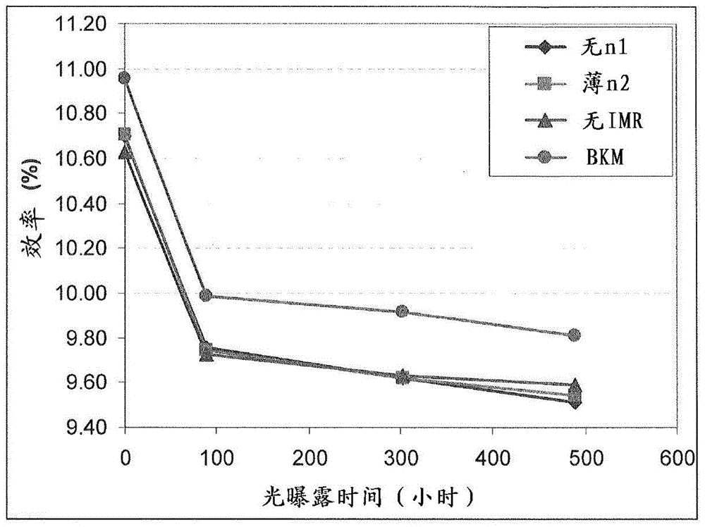
[0083] The present invention proposes to modify the prior art n-layer 54 into a multilayer structure 64-67. Two n-layer structures were found to be the optimal solution with regard to the highest initial and stable amorphous microcrystalline module power (BKM). The layer deposition sequence described below starts after the deposition of the amorphous i layer 63 . Variations 3A and 3B are combined with additional steps for forming the two BKMs respectively:

[0084] 1. Deposit an n-layer (n1, 64) of amorphous silicon


PUM

PropertyMeasurementUnit
Thicknessaaaaaaaaaa
Thicknessaaaaaaaaaa
Thicknessaaaaaaaaaa

Abstract

The invention relates to a multijunction thin film solar cell (70) of high efficiency and low-cost production. The n-layer (64, 65, 66, 67) of one of the constituent cells (61) of the multijunction thin film solar cell has a structure comprising, in the intended direction of impinging light, a sequence of an amorphous hydrogenated silicon n-layer (64), a first microcrystalline hydrogenated silicon n-layer (65), an intermediate reflector layer (66) and a second microcrystalline hydrogenated silicon n-layer (67), wherein the intermediate reflector layer is one of the following: - a single microcrystalline essentially silicon oxide layer; or - a plurality of layer sequences, each layer sequence consisting of a microcrystalline essentially silicon oxide layer and a microcrystalline silicon n-layer in the intended direction of impinging light. The invention further relates to methods of manufacturing the above n-layer (64, 65, 66, 67), and to methods of manufacturing the above-mentioned multijunction thin film solar cell (70).

Description


Claims


Application Information

Patent Timeline
Owner TEL太阳能公司
Why Eureka
Try Eureka