Back-illuminated image sensor with three-dimensional transistor structure and forming method thereof
An image sensor and transistor technology, applied in the field of image sensors, can solve the problems of difficulty in the fabrication of gate structures of transistors, and achieve the effects of improving ConversionGain, improving transconductance, and increasing filling rate.
- Summary
- Abstract
- Description
- Claims
- Application Information
AI Technical Summary
Benefits of technology
Problems solved by technology
Method used
Image

Examples
Embodiment Construction
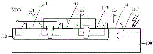
[0033] In existing image sensors, transistors (such as source follower transistors, transfer transistors, and reset transistors, etc.) are usually planar structures. Therefore, the corresponding pixel units have many defects. For example, it is difficult to further reduce the chip area of image sensors. The cost remains high, the image quality formed by the image sensor is difficult to further improve, the noise level of the image sensor is difficult to reduce, and the area occupancy rate of the photoelectric conversion element in the pixel unit is difficult to increase.
[0034] In existing image sensors, 3D transistors may be used in the process design of image sensors, but during the formation of the gate region of the transistor, the polysilicon etching of the gate region is difficult to control, resulting in the performance of the formed gate region Not good, poor interface goodness.
[0035] The present invention provides a method for forming a back-illuminated image sens
PUM
 Abstract
Description
Claims
Application Information
 - R&D Engineer
- R&D Manager
- IP Professional
- Industry Leading Data Capabilities
- Powerful AI technology
- Patent DNA Extraction
Browse by: Latest US Patents, China's latest patents, Technical Efficacy Thesaurus, Application Domain, Technology Topic.
© 2024 PatSnap. All rights reserved.Legal|Privacy policy|Modern Slavery Act Transparency Statement|Sitemap