Thin-film sputtering force transducer adapting to lunar environment
A technology of force sensor and sensor unit, applied in the field of thin film sputtering force sensor, to achieve the effects of light weight, light weight, high stability and test accuracy
- Summary
- Abstract
- Description
- Claims
- Application Information
AI Technical Summary
Benefits of technology
Problems solved by technology
Method used
Image

Examples
Embodiment Construction
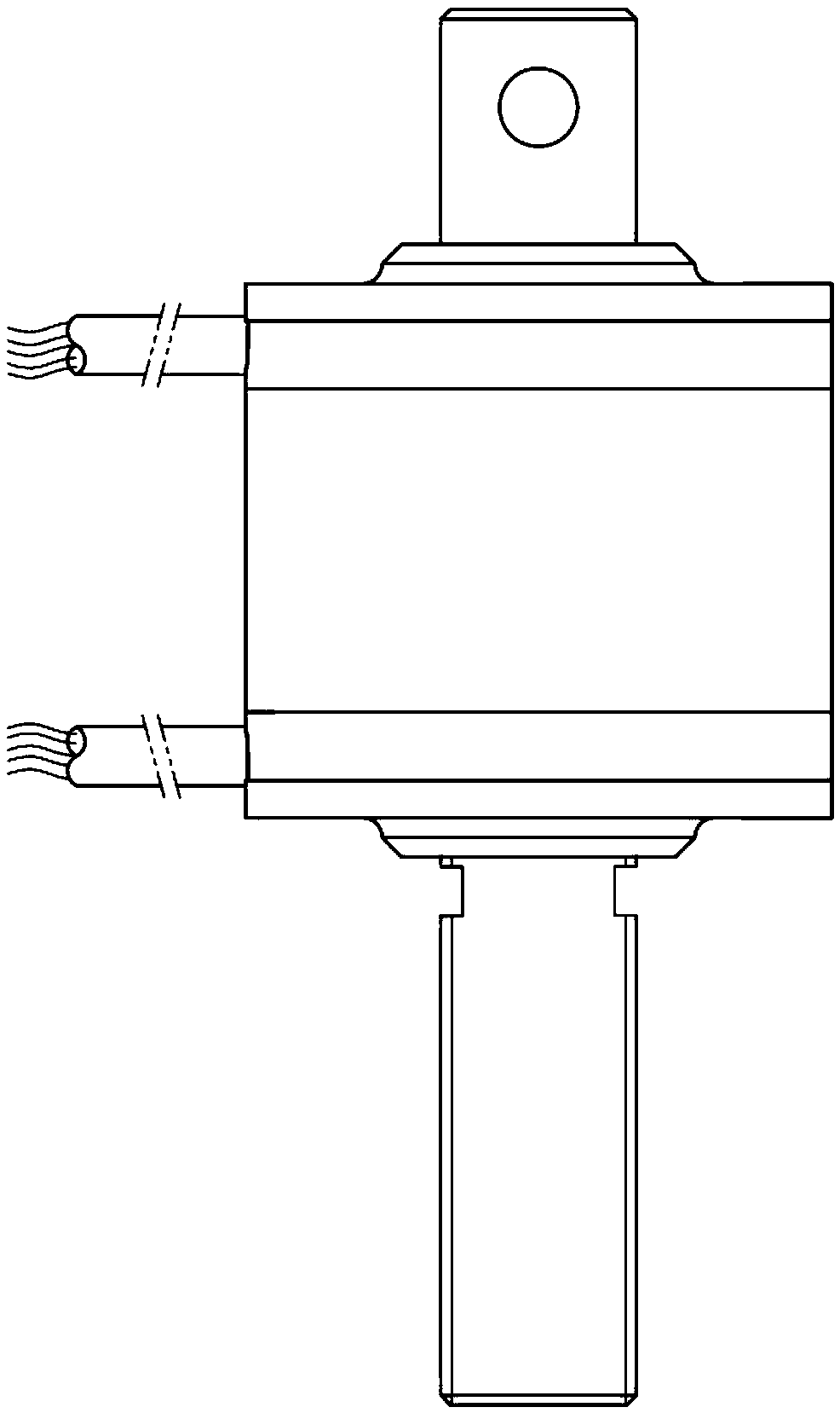
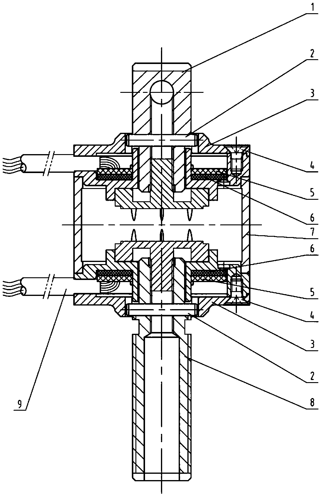
[0049] Such as figure 1 and figure 2 As shown, the thin film sputtering force sensor of the present invention includes a sensor component 7 .
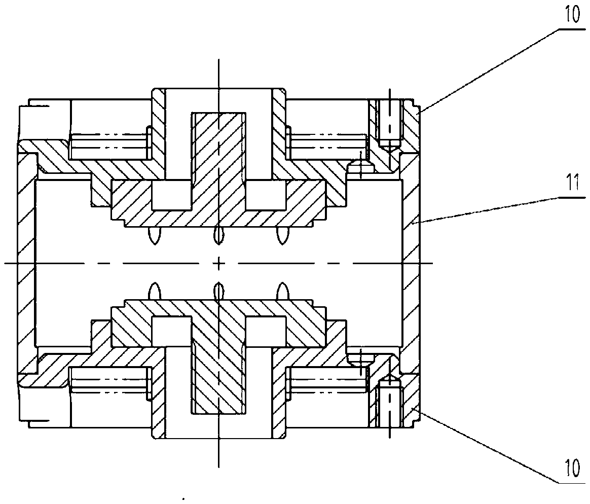
[0050] Such as image 3 As shown, the sensor assembly 7 includes a sensor unit 10 and a housing 11 .
[0051] Such as figure 2 , Figure 4 and Figure 5 As shown, the sensor unit 10 is composed of a connection end, a cylindrical pin 2, an end cover 3, a cross-recessed countersunk screw 4, a circuit board 5, a circuit board protection pad 6, a cable 9, a terminal block 12, a lead terminal insulating seat 13, a lead wire The pin 14, the bonding gold wire 15 and the elastic body 16 are composed.
[0052] Such as Figure 8 As shown, the elastic body 16 is a convex-shaped stepped cylindrical platform, including a thick cylindrical platform and a thin cylindrical platform. direction deformation, and reduce the weight of the elastic body 16; the terminal block 12 is a rotating body, coaxial with the elastic body 16, the terminal block
PUM
| Property | Measurement | Unit |
|---|---|---|
| Radian | aaaaa | aaaaa |
| Radian | aaaaa | aaaaa |
Abstract
Description
Claims
Application Information
 - R&D Engineer
- R&D Manager
- IP Professional
- Industry Leading Data Capabilities
- Powerful AI technology
- Patent DNA Extraction
Browse by: Latest US Patents, China's latest patents, Technical Efficacy Thesaurus, Application Domain, Technology Topic.
© 2024 PatSnap. All rights reserved.Legal|Privacy policy|Modern Slavery Act Transparency Statement|Sitemap