Preparation method of LED chip and LED chip prepared by adopting method

A technology of LED chips and anti-reflection coatings, applied in electrical components, circuits, semiconductor devices, etc., can solve the problems that the ITO transparent conductive layer is easily damaged and polluted, and affect the brightness of LEDs, so as to reduce the risk of the current blocking layer and avoid Damage and contamination, the effect of avoiding harm

Inactive Publication Date: 2016-10-12
XIANGNENG HUALEI OPTOELECTRONICS
View PDF5 Cites 5 Cited by
  • Summary
  • Abstract
  • Description
  • Claims
  • Application Information

AI Technical Summary

Problems solved by technology

[0006] The purpose of the present invention is to provide a method for preparing an LED chip and the LED chip prepared by the method, so as to solve the problem that the ITO transparent conductive layer is easily damaged and polluted in the existing LED chip manufacturing process and thus affects the brightness of the LED. The preparation method of the LED chip is to deposit a SiON anti-reflection film on the sur

Method used


Image

  • Preparation method of LED chip and LED chip prepared by adopting method
  • Preparation method of LED chip and LED chip prepared by adopting method
  • Preparation method of LED chip and LED chip prepared by adopting method

Examples


Embodiment Construction

[0031] The embodiments of the present invention will be described in detail below with reference to the accompanying drawings, but the present invention can be implemented in various ways defined and covered by the claims.

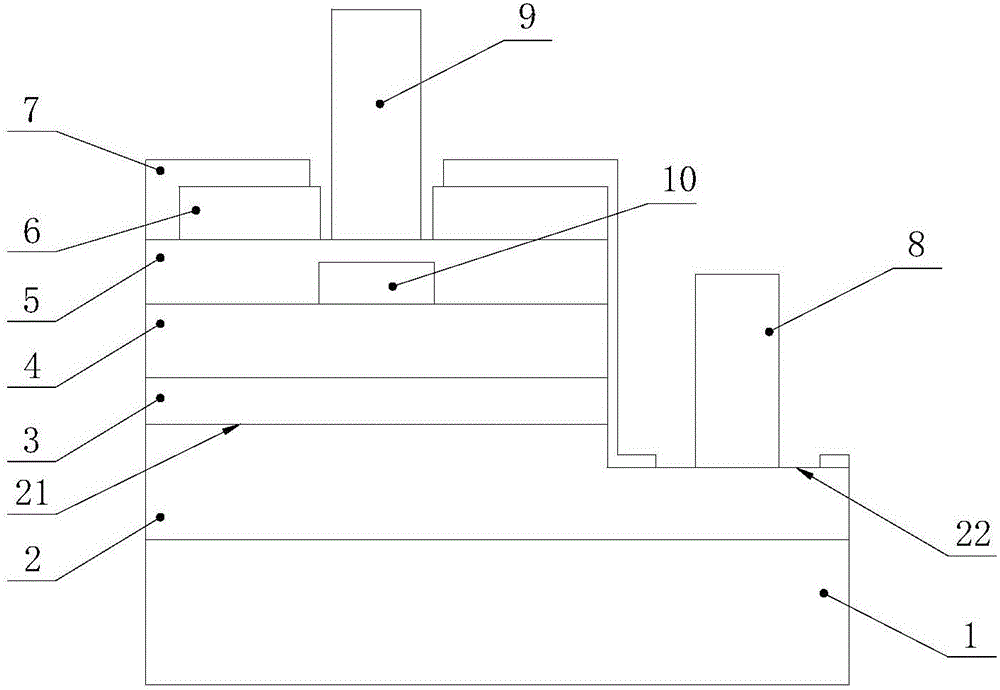
[0032] see figure 1 , a kind of LED chip of the present invention, this LED chip comprises substrate 1, epitaxial layer and electrode successively in thickness direction, and epitaxial layer comprises N-type semiconductor layer 2, light emitting layer 3 and P-type semiconductor layer 4, N-type semiconductor layer 2 is a stepped structure including an upper stepped portion 21 and a lower stepped portion 22, the light emitting layer 3 and the P-type semiconductor layer 4 are sequentially arranged above the upper stepped portion 21, and an ITO transparent conductive layer is also provided on the P-type semiconductor layer 4 5. The electrodes include an N electrode 8 arranged on the lower step portion 22 and a P electrode 9 arranged on the ITO transparent conduct


PUM

PropertyMeasurementUnit
Thicknessaaaaaaaaaa

Abstract

The invention provides a preparation method of an LED chip and an LED chip prepared by adopting the method. The LED chip comprises an N-type semiconductor layer, a light emitting layer, a P-type semiconductor layer, a current blocking layer and an ITO (Indium Tin Oxide) transparent conducting layer covered on the current blocking layer, and is characterized in that the N-type semiconductor layer, the light emitting layer, the P-type semiconductor layer, the current blocking layer and the ITO transparent conducting layer sequentially grow on a substrate, an N electrode is prepared on the N-type semiconductor layer, a P electrode is prepared on the ITO transparent conducting layer, an SiO2 protection layer is deposited at the upper surface of the chip at the outer side of the N electrode, and an SiON anti-reflection film and an SiO2 protection layer are sequentially deposited at the upper surface of the chip at the outer side of the P electrode. According to the invention, the SiON anti-reflection film is deposited at the surface of the ITO transparent conducting layer, and the SiON anti-reflection film is etched by using a phosphoric acid solution, thereby preventing the ITO transparent conducting film from being damaged or polluted in the manufacturing process of the chip, improving the quality of the ITO transparent conducting layer, enabling the chip voltage to be reduced while improving the brightness of the LED chip, and enabling an LED to be more energy-saving and more environment-friendly.

Description


Claims


Application Information

Patent Timeline
Owner XIANGNENG HUALEI OPTOELECTRONICS
Why Eureka
Try Eureka