Printed circuit board element for forming enhancement mode biosensing module and fabrication method for printed circuit board element

A printed circuit board and bio-sensing technology, which is applied to printed circuits, printed circuits connected with non-printed electrical components, electrical components, etc., can solve problems such as structural deformation of the module's mechanical weaknesses, and achieve simple and reasonable structural design. Avoid the effect of cracking

Inactive Publication Date: 2017-05-17
SUNASIC TECH
View PDF9 Cites 3 Cited by
  • Summary
  • Abstract
  • Description
  • Claims
  • Application Information

AI Technical Summary

Benefits of technology

This patented technical effect of this patents describes an improved biological sensor chip that includes a specialized part made up of tiny electrically-conducted parts called pads on its top face. These small parts help prevent damage from external factors like impacts during transportation without adding extra weight compared with traditional sensors used at home. Additionally, these chips have very low costs due to their use of less expensive materials instead of heavy metals.

Problems solved by technology

This technical problem addressed in this patents relates to integrating electrical elements within a small space without causing any issues related to their functionality. Existing techniques involve embedding them inside packages containing various layers, but they have drawbacks due to factors like manufacture variations caused by environmental conditions.

Method used


Image

  • Printed circuit board element for forming enhancement mode biosensing module and fabrication method for printed circuit board element
  • Printed circuit board element for forming enhancement mode biosensing module and fabrication method for printed circuit board element
  • Printed circuit board element for forming enhancement mode biosensing module and fabrication method for printed circuit board element

Examples


Embodiment Construction

[0064] In order to make the object, technical solution and advantages of the present invention clearer, the printed circuit board component for forming the enhanced biosensor module and the manufacturing method thereof of the present invention will be further described in detail through the following embodiments in conjunction with the accompanying drawings. It should be understood that the specific embodiments described here are only used to explain the present invention, not to limit the present invention.

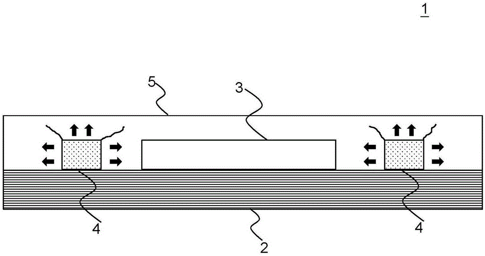
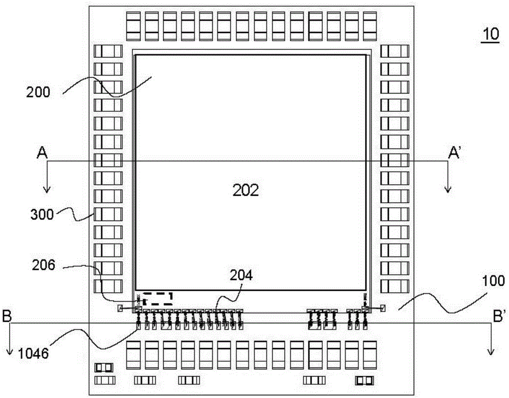
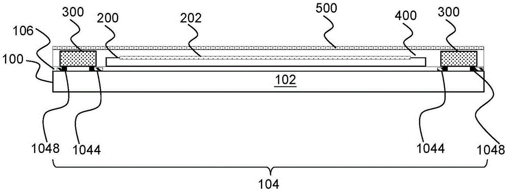
[0065] In one embodiment of the present invention, see Figure 2 to Figure 5 , the printed circuit board component 10 forms an enhanced biosensing module. See also Figure 2 to Figure 4 . figure 2 is a top view of the printed circuit board component 10, image 3 for printed circuit board components along with 10 figure 2 The sectional view of the line AA' in the middle, Figure 4 is a cross-sectional view of the printed circuit board component 10 along line BB'. The


PUM


Abstract

The invention provides a printed circuit board element for forming an enhancement mode biosensing module and a fabrication method for the printed circuit board element. The printed circuit board element comprises a printed circuit board, a biosensing chip and a protection layer, wherein the printed circuit board comprises an insulating layer and a conductive layer; the conductive layer forms a working circuit, an excitation circuit, multiple first connecting point welding pads and multiple second connecting point welding pads on a part of the upper surface of the insulating layer, wherein the second connecting point welding pads are connected to the excitation circuit; the biosensing chip is assembled on the printed circuit board; the biosensing chip comprises a sensing region, an excitation signal source, multiple combination welding pads and multiple conductive elements; each combination welding pad is electrically connected to the corresponding first connecting point welding pad; the excitation signal source is connected to the excitation circuit through the combination welding pads and used for providing an excitation signal; each conductive element is assembled on the corresponding second connecting point welding pad; and the protection layer is formed on and covers the printed circuit board, the biosensing chip and the conductive elements. According to the printed circuit board element, cracking of the protection layer can be avoided by virtue of the light and thin dimensions of the conductive elements.

Description


Claims


Application Information

Patent Timeline
Owner SUNASIC TECH
Why Eureka
Try Eureka