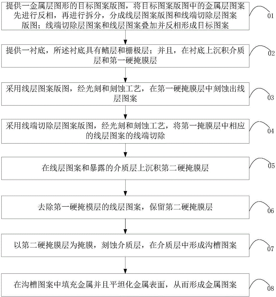
Method for preparing metal pattern for fin field effect transistor
A fin field effect and metal pattern technology, applied in semiconductor/solid-state device manufacturing, semiconductor devices, electrical components, etc., can solve the problems of affecting device performance and the effect of the connection between the metal layer zero and the fin layer, etc. The effect of large in-line process window, improved connection performance, improved device yield and reliability
- Summary
- Abstract
- Description
- Claims
- Application Information
AI Technical Summary
Benefits of technology
Problems solved by technology
Method used
Image

Examples
Embodiment Construction
[0030] In order to make the content of the present invention clearer and easier to understand, the content of the present invention will be further described below in conjunction with the accompanying drawings. Of course, the present invention is not limited to this specific embodiment, and general replacements known to those skilled in the art are also covered within the protection scope of the present invention.
[0031] The following is attached Figure 1-13 The present invention will be described in further detail with specific examples. It should be noted that the drawings are all in a very simplified form, using imprecise scales, and are only used to facilitate and clearly achieve the purpose of assisting in describing the present embodiment.
[0032] For the preparation method of a fin field effect transistor metal pattern in this embodiment, please refer to figure 1 , including:
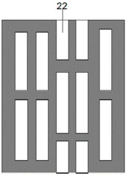
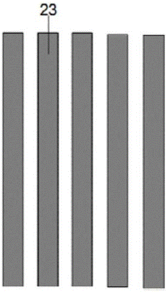
[0033] Step 01: See Figure 2~4 , providing a target pattern layout of a metal layer pat
PUM
 Abstract
Description
Claims
Application Information
 - R&D Engineer
- R&D Manager
- IP Professional
- Industry Leading Data Capabilities
- Powerful AI technology
- Patent DNA Extraction
Browse by: Latest US Patents, China's latest patents, Technical Efficacy Thesaurus, Application Domain, Technology Topic.
© 2024 PatSnap. All rights reserved.Legal|Privacy policy|Modern Slavery Act Transparency Statement|Sitemap