Hall component and fabrication method thereof
A technology of Hall elements and doping elements, applied in the semiconductor field, can solve problems such as poor temperature drift characteristics, achieve low temperature drift, improve reliability, and simplify applications
- Summary
- Abstract
- Description
- Claims
- Application Information
AI Technical Summary
Problems solved by technology
Method used
Image

Examples
Embodiment 1
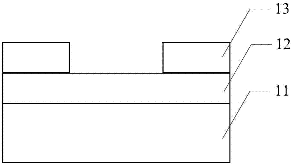
[0027] This embodiment provides a Hall element, such as figure 1 As shown, it includes a stacked substrate layer 11, a semiconductor functional layer 12 and an electrode layer 13; the semiconductor functional layer 12 is N-type doped In x Ga 1-x As 1-2x P 2x layer, where the value of x is greater than 0 and not greater than 0.5. In x Ga 1-x As 1-2x P 2x The material is lattice matched to the gallium arsenide substrate. in x Ga 1-x As 1-2x P 2x N-type semiconductors are formed after doping with pentavalent elements. Since free electrons are mainly provided by impurity atoms, the more impurities are doped, the higher the concentration of many sons (free electrons), and the stronger the conductivity.
[0028] As an optional implementation, In x Ga 1-x As 1-2x P 2x The doped pentavalent element in the layer is at least one of tellurium (Te), selenium (Se), sulfur (S), silicon (Si), tin (Sn), germanium (Ge), and the doping concentration is 3 ×10 16 cm -3 to 3×10 17
Embodiment 2
[0039] This embodiment provides a Hall element, the structure is the same as Embodiment 1, the difference is that the value of x is 0.5, that is, the semiconductor functional layer is In 0.5 Ga 0.5 P, the doping element is tellurium, and the doping concentration is 3×10 16 cm -3 , with a thickness of 0.5 μm.
Embodiment 3
[0041] This embodiment provides a Hall element, the structure is the same as that of Embodiment 1, the difference is that the value of x is 0.1, that is, the semiconductor functional layer is In 0.1 Ga 0.9 As 0.8 P 0.2 , the doping element is germanium, and the doping concentration is 8×10 16 cm -3 , with a thickness of 0.1 μm.
PUM
| Property | Measurement | Unit |
|---|---|---|
| Thickness | aaaaa | aaaaa |
| Thickness | aaaaa | aaaaa |
Abstract
Description
Claims
Application Information
 - R&D Engineer
- R&D Manager
- IP Professional
- Industry Leading Data Capabilities
- Powerful AI technology
- Patent DNA Extraction
Browse by: Latest US Patents, China's latest patents, Technical Efficacy Thesaurus, Application Domain, Technology Topic.
© 2024 PatSnap. All rights reserved.Legal|Privacy policy|Modern Slavery Act Transparency Statement|Sitemap