Printed circuit board soldering protection nail bed and manufacturing method thereof

A printed circuit board and nail bed technology, which is applied in the fields of printed circuit manufacturing, printed circuit, and printed circuit secondary processing, can solve the problems of difficult management, error-prone, high nail bed processing costs, etc., to reduce management difficulty and improve Work efficiency, material cost saving effects

Active Publication Date: 2018-02-16
广东喜珍电路科技有限公司
View PDF5 Cites 2 Cited by
  • Summary
  • Abstract
  • Description
  • Claims
  • Application Information

AI Technical Summary

Benefits of technology

This patented technology allows for easy re-use or replacement of used boards with new ones without requiring expensive equipment such as drills, scrapers, or tape measures. It also helps save materials costs while producing more efficient work processes compared to traditional methods like welding.

Problems solved by technology

This patented technical problem addressed in this patents relates to providing an improved antisticking nailbed for printed circuits without requiring complicated processes like fixing screw bolts during fabricating them. Additionally, current methods may cause issues due to poor accuracy caused by incorrect placement of positioning pins and lack of space available around specific areas where solder paste cannot attach properly onto the substrate.

Method used


Image

  • Printed circuit board soldering protection nail bed and manufacturing method thereof
  • Printed circuit board soldering protection nail bed and manufacturing method thereof
  • Printed circuit board soldering protection nail bed and manufacturing method thereof

Examples


Embodiment Construction

[0033] The present invention will be further described below in conjunction with the accompanying drawings and embodiments.

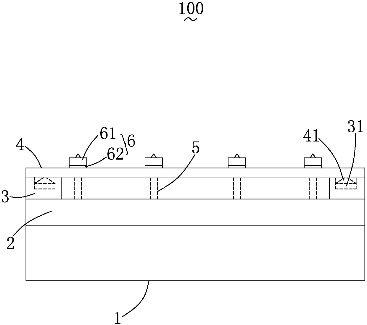
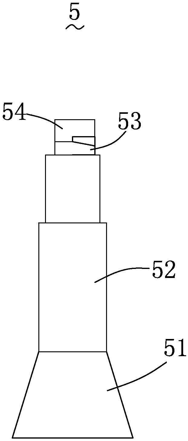
[0034] see figure 1 , is a structural schematic diagram of a preferred embodiment of a printed circuit board solder resist nail bed provided by the present invention. The printed circuit board anti-soldering nail bed 100 includes a support frame 1, a first nail bed bottom plate 2 carried by the support frame 1, and a support frame plate 3 ring-shaped on the top outer peripheral surface of the first nail bed bottom plate 2 , the second nail bed bottom plate 4 erected on the top of the support frame plate 3, the adsorption assembly 5 sandwiched between the first nail bed bottom plate 2 and the second nail bed bottom plate 4, and the second nail bed bottom plate 4 Several PIN nails 6 on the surface of the bed of nails bottom plate 4, the circuit system 7 and the LCD screen display electrically connected with the adsorption assembly 5.

[0035] The first nai


PUM

PropertyMeasurementUnit
Thicknessaaaaaaaaaa

Abstract

The invention provides a printed circuit board soldering protection nail bed and a manufacturing method thereof. The printed circuit board soldering protection nail bed comprises a support frame, a first nail bed bottom plate supported by the support frame, a support frame plate annularly arranged on the peripheral surface of the top of the first nail bed bottom plate, a second nail bed bottom plate erected at the top of the support frame plate, an adsorption assembly sandwiched between the first nail bed bottom plate and the second nail bed bottom plate, a plurality of PINs arranged on the surface of the second nail bed bottom plate and a circuit system electrically connected with the adsorption assembly. The above structure can solve the problem about rapid and repeated use of the nail bed plates and the PINs, the nail bed can be manufactured rapidly without a drilling machine, a drill belt and an adhesive tape, meanwhile, the material cost, manufacturing cost and management cost forthe nail bed are saved, the storage space for the nail bed bottom plates is reduced, the difficulty of management is reduced, the nail bed is convenient to use, and the working efficiency is improved.

Description


Claims


Application Information

Patent Timeline
Owner 广东喜珍电路科技有限公司
Why Eureka
Try Eureka