Nanotube memory structure and preparation method thereof

A nanotube and memory technology, which is applied to the nanotube memory structure and the field of its preparation, can solve the problems of difficulty in taking into account processes and affect product yield, and achieve the effects of easy control of the preparation process, high product yield, and simplified device structure.

Active Publication Date: 2018-03-06
ZING SEMICON CORP
View PDF1 Cites 4 Cited by
  • Summary
  • Abstract
  • Description
  • Claims
  • Application Information

AI Technical Summary

Benefits of technology

This technology allows for more efficient use of space by storing data into multiple layers within one transistor chip instead of just two or three separate chips connected together through wires. It also simplifies its production processes while maintaining their effectiveness at higher levels of integration density compared to previous designs that had many connections between different parts.

Problems solved by technology

This patented technical problem addressed in this patents relates to improving the performance and efficiency of current vertically channel type triple-level cell (TSC) devices due to their limitations in terms of reducing transistor size while maintaining sufficient space inside them without sacrificially increasing manufacturing costs. Current methods involve depositing films like polycide over active areas, forming channels around these structures, and filling gaps within those structures with insulating layers containing charges. These techniques have resulted in decreased planarization capabilities compared to other types of memory systems.

Method used


Image

  • Nanotube memory structure and preparation method thereof
  • Nanotube memory structure and preparation method thereof
  • Nanotube memory structure and preparation method thereof

Examples


Embodiment Construction

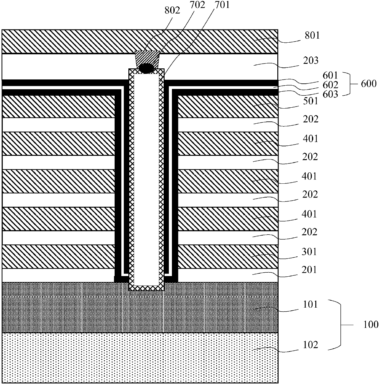
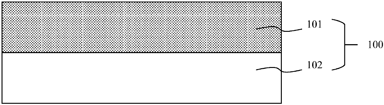
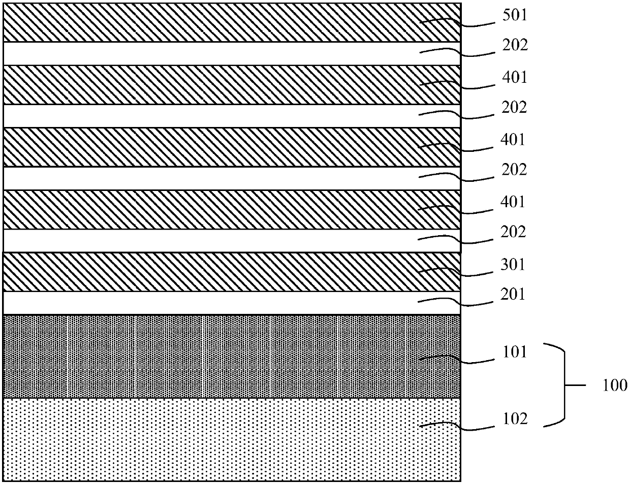
[0078] Embodiments of the present invention are described below through specific examples, and those skilled in the art can easily understand other advantages and effects of the present invention from the content disclosed in this specification. The present invention can also be implemented or applied through other different specific implementation modes, and various modifications or changes can be made to the details in this specification based on different viewpoints and applications without departing from the spirit of the present invention. It should be noted that, in the case of no conflict, the following embodiments and features in the embodiments can be combined with each other.

[0079] It should be noted that the diagrams provided in the following embodiments are only schematically illustrating the basic ideas of the present invention, and only the components related to the present invention are shown in the diagrams rather than the number, shape and shape of the componen


PUM

PropertyMeasurementUnit
Doping concentrationaaaaaaaaaa
Thicknessaaaaaaaaaa
Widthaaaaaaaaaa

Abstract

The invention provides a nanotube memory structure and a preparation method thereof. The nanotube memory structure comprises the components of a semiconductor substrate with a heavily doped epitaxiallayer on the surface; a first isolating dielectric layer, a ground selecting gate electrode layer, a bit line gate electrode layer, a string selecting gate electrode layer, and multiple second isolating dielectric layers among the ground selecting gate electrode layer, the bit line gate electrode layer and the string selecting gate electrode layer, wherein the first isolating dielectric layer, theground selecting gate electrode layer, the bit line gate electrode layer, the string selecting gate electrode layer and the multiple second isolating dielectric layers are arranged on the semiconductor substrate; a semiconductor channel which penetrates through the ground selecting gate electrode layer, the bit line gate electrode layer and the string selecting gate electrode layer; and a gate electrode dielectric layer which packages the sidewall of the semiconductor channel, wherein the semiconductor channel is a semiconductor nanotube on the heavily doped epitaxial layer. According to thememory structure, the semiconductor nanotube which epitaxially grows on the heavily doped epitaxial layer is used as the vertical channel; and compared with an existing vertical channel type NAND structure, the nanotube memory structure has advantages of further simplified device structure, easy controlling for the preparation process, and high yield rate of products.

Description


Claims


Application Information

Patent Timeline
Owner ZING SEMICON CORP
Why Eureka
Try Eureka