Method for measuring organic magnetic resistance of organic semiconductors

An organic semiconductor and magnetoresistance technology, applied in the direction of measuring magnetic variables, measuring devices, instruments, etc., to achieve the effect of simple operation

Inactive Publication Date: 2018-12-21
INST OF MICROELECTRONICS CHINESE ACAD OF SCI
View PDF4 Cites 0 Cited by
  • Summary
  • Abstract
  • Description
  • Claims
  • Application Information

AI Technical Summary

Problems solved by technology

[0005] The present invention aims to provide a simple method for measuring the organic magnetoresistance of organic semiconductors to solve the problem tha

Method used


Image

  • Method for measuring organic magnetic resistance of organic semiconductors
  • Method for measuring organic magnetic resistance of organic semiconductors
  • Method for measuring organic magnetic resistance of organic semiconductors

Examples


Embodiment Construction

[0037] In order to make the purpose, technical solution and advantages of the present invention clearer, the technical solution of the present invention will be clearly and completely described below in conjunction with the accompanying drawings of the embodiments of the present invention. Apparently, the described embodiment is one embodiment of the present invention, but not all of them. Based on the described embodiments of the present invention, all other embodiments obtained by persons of ordinary skill in the art without creative efforts shall fall within the protection scope of the present invention.

[0038] Unless otherwise defined, the technical terms or scientific terms used in the present invention shall have the usual meanings understood by those skilled in the art to which the present invention belongs.

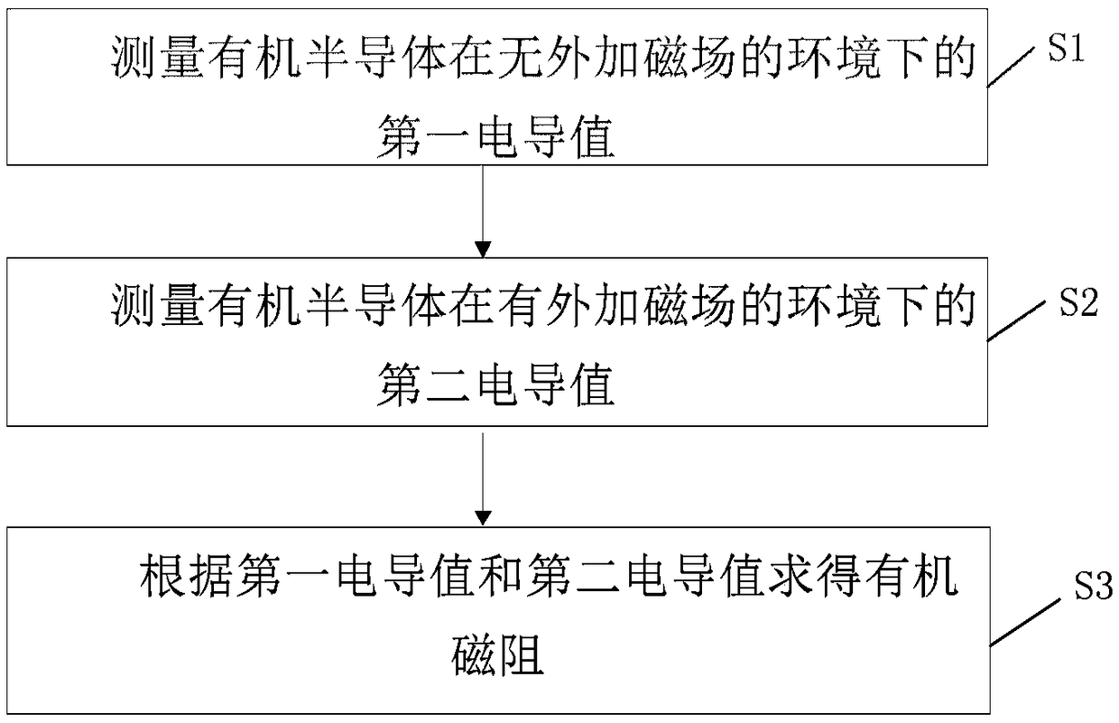
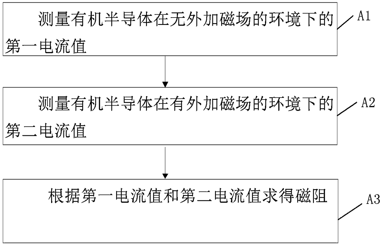
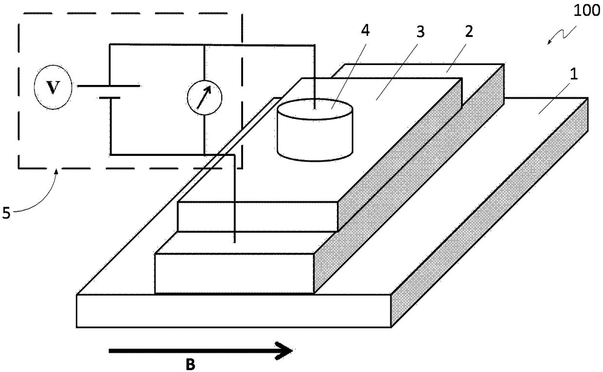
[0039] Such as figure 1 As shown, an embodiment of the present invention provides a method for measuring the organic magnetoresistance of an organic semiconductor


PUM


Abstract

The invention discloses a method for measuring organic magnetic resistance of organic semiconductors. The method comprises the steps that first conductance values of the organic semiconductors under the environment without applied magnetic fields are measured; second conductance values of the organic semiconductors under the environment of the applied magnetic fields are measured; and the organicmagnetic resistance is obtained according to the first conductance values and the second conductance values. Through the disclosed method, the magnetic resistance of different organic semiconductor materials can be obtained easily and accurately, then the organic magnetic resistance effects of different organic material devices under different temperatures, electric field intensity, magnetic fields and carrier concentrations can be obtained, and the universal physical method is provided for studying microphysical mechanisms of the different types of organic magnetic resistance devices.

Description


Claims


Application Information

Patent Timeline
Owner INST OF MICROELECTRONICS CHINESE ACAD OF SCI
Why Eureka
Try Eureka