Display substrate and manufacturing method thereof, and display device

A technology for a display substrate and a manufacturing method, which is applied in the fields of semiconductor/solid-state device manufacturing, electrical components, and electrical solid-state devices, etc., can solve the problems of increasing the frame of OLED devices, unfavorable narrow frame of OLED devices, and reducing the yield of OLED devices, etc. Achieve the effect of reducing the frame, improving the yield, and avoiding short circuits

Active Publication Date: 2019-03-26
BOE TECH GRP CO LTD
View PDF3 Cites 1 Cited by
  • Summary
  • Abstract
  • Description
  • Claims
  • Application Information

AI Technical Summary

Problems solved by technology

Among them, the sputtering process is usually used to prepare the cathode covering the entire layer of the display area. However, when preparing the cathode in the prior art, the cathode formed by sputtering often exceeds the display area. On the one hand, short circuits are prone to occur, which reduces the yield of OLED devices; On the one hand, the frame of the OLED device will become larger, which is not conducive to the realization of a narrow frame of the OLED device

Method used


Image

  • Display substrate and manufacturing method thereof, and display device
  • Display substrate and manufacturing method thereof, and display device
  • Display substrate and manufacturing method thereof, and display device

Examples


Example Embodiment

[0035] In order to make the technical problems, technical solutions and advantages to be solved by the embodiments of the present invention clearer, the following detailed description will be given in conjunction with the accompanying drawings and specific embodiments.

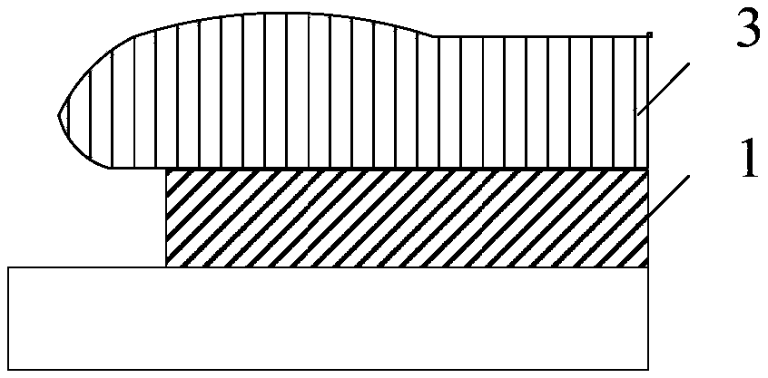
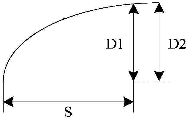
[0036] The embodiments of the present invention are aimed at preparing the cathode in the prior art, the cathode formed by sputtering often exceeds the display area, on the one hand, short circuit is prone to occur, which reduces the yield of the OLED device; on the other hand, the frame of the OLED device becomes larger. , which is not conducive to the realization of the narrow frame of the OLED device, and provides a display substrate, a manufacturing method thereof, and a display device, which can improve the yield of the display substrate and at the same time facilitate the realization of the narrow frame of the display device.

[0037] Embodiments of the present invention provide a method for fabricating a di


PUM


Abstract

The invention, which belongs to the technical field of display, provides a display substrate and a manufacturing method thereof, and a display device. The manufacturing method comprises the followingsteps that: a deformable film layer covering a non-display area of a display substrate is formed, wherein the deformable film layer includes a hollow-out part corresponding to a display area of the display substrate; an overall electrode layer is formed on the display substrate with the deformable film layer formed; the size of the deformable film layer is increased and thus the electrode layer part formed on the deformable film layer is separated from the electrode layer part formed in the display area naturally; and the deformable film layer is removed from the display substrate. Therefore,the yield of the display substrate is improved; and the narrow frame of the display device is realized.

Description


Claims


Application Information

Patent Timeline
Owner BOE TECH GRP CO LTD
Why Eureka
Try Eureka