Automatic high speed exposure device and method for circuit board
An exposure method and circuit board technology, which are applied in the field of circuit board manufacturing, can solve problems such as inability to meet circuit boards, and achieve the effects of simplifying structure, improving exposure efficiency, and reducing production costs.
- Summary
- Abstract
- Description
- Claims
- Application Information
AI Technical Summary
Problems solved by technology
Method used
Image

Examples
Example Embodiment
[0043] The following will clearly and completely describe the technical solutions in the embodiments of the present invention with reference to the accompanying drawings in the embodiments of the present invention. Obviously, the described embodiments are only some, not all, embodiments of the present invention. Based on the embodiments of the present invention, all other embodiments obtained by persons of ordinary skill in the art without making creative efforts belong to the protection scope of the present invention.
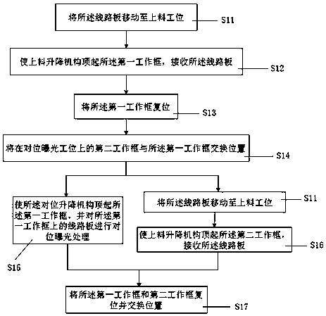
[0044] figure 1 It is a flowchart of a fully automatic high-speed exposure method for circuit boards in an embodiment of the present invention, and the fully automatic high-speed exposure method for circuit boards includes the following steps S11-S17.
[0045] S11. Moving the circuit board to a loading station.
[0046] S12. Make the feeding lifting mechanism lift up the first working frame to receive the circuit board. Wherein, the first working frame includes
PUM
 Abstract
Description
Claims
Application Information
 - R&D Engineer
- R&D Manager
- IP Professional
- Industry Leading Data Capabilities
- Powerful AI technology
- Patent DNA Extraction
Browse by: Latest US Patents, China's latest patents, Technical Efficacy Thesaurus, Application Domain, Technology Topic.
© 2024 PatSnap. All rights reserved.Legal|Privacy policy|Modern Slavery Act Transparency Statement|Sitemap