Electrical fire monitoring system based on photoelectric film chip
A thin-film chip and electrical fire technology, which is applied to electrical components, fire alarms, circuits, etc., can solve the problems of increasing the complexity and manufacturing cost of detectors, reducing the scope of application of detectors, and being fragile and expensive, so as to achieve sensitive response , stable performance and simple operation
- Summary
- Abstract
- Description
- Claims
- Application Information
AI Technical Summary
Benefits of technology
Problems solved by technology
Method used
Image

Examples
Embodiment 1
[0025] A method for making an electrical fire monitoring system based on a photoelectric thin film chip has the following steps:
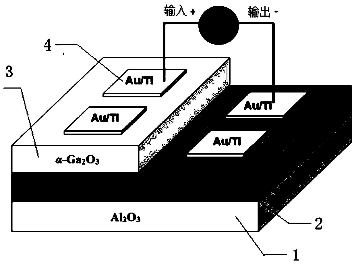
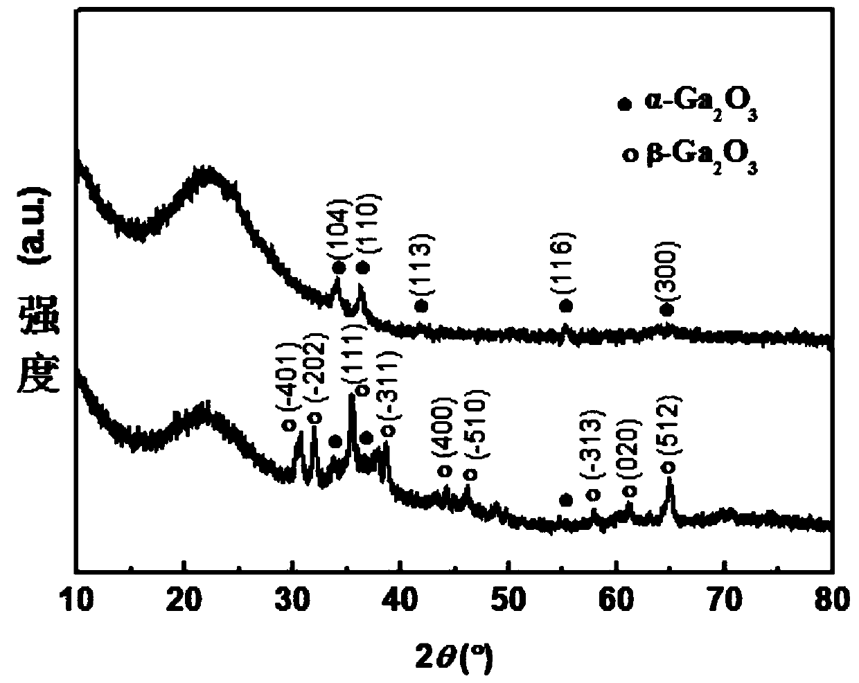
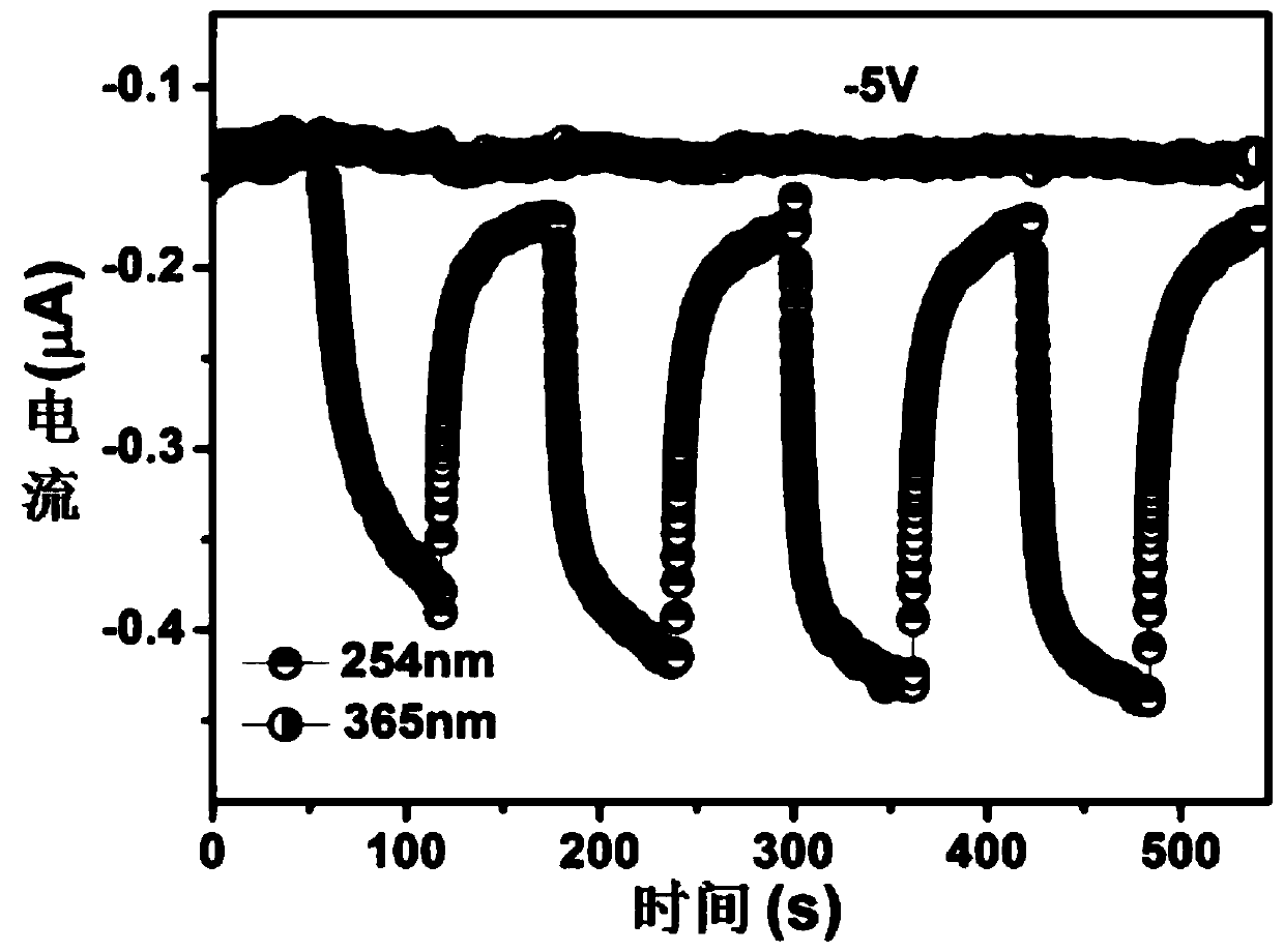
[0026] (1)α-Ga 2 o 3 / β-Ga 2 o 3 Fabrication of the junction thin film chip:
[0027] Put the sapphire substrate into V(HF):V(H 2 o 2 )=1:5 solution soaked to remove the natural oxide layer, then ultrasonic cleaning with acetone, ethanol and deionized water, and vacuum drying; the Ga 2 o 3The target is placed on the target stage of the magnetron sputtering system, the sapphire substrate after the above treatment is fixed on the sample holder, and put into the vacuum chamber; the chamber is first vacuumed, and argon and oxygen are introduced to adjust the vacuum chamber The internal pressure, heating the sapphire substrate, opening the target baffle, and growing β-Ga 2 o 3 thin film, after the growth of the thin film is completed, oxygen is introduced, the pressure in the vacuum chamber is adjusted, and the obtained β-Ga 2 o 3 The thin fil
Embodiment 2
[0036] Step (2) is identical with embodiment 1. Put the sapphire substrate into V(HF):V(H 2 o 2 )=1:5 solution soaked to remove the natural oxide layer, then ultrasonic cleaning with acetone, ethanol and deionized water, and vacuum drying; the Ga 2 o 3 The target is placed on the target stage of the magnetron sputtering system, the sapphire substrate after the above treatment is fixed on the sample holder, and put into the vacuum chamber; the chamber is first vacuumed, and argon and oxygen are introduced to adjust the vacuum chamber The internal pressure, heating the sapphire substrate, opening the target baffle, and growing β-Ga 2 o 3 thin film, after the growth of the thin film is completed, oxygen is introduced, the pressure in the vacuum chamber is adjusted, and the obtained β-Ga 2 o 3 The thin film is annealed in situ; among them, Ga 2 o 3 The distance between the target and the sapphire substrate was set at 5 cm, and the chamber pressure after vacuuming was 1×10 -6
Embodiment 3
[0040] Step (2) is identical with embodiment 1. Put the sapphire substrate into V(HF):V(H 2 o 2 )=1:5 solution soaked to remove the natural oxide layer, then ultrasonic cleaning with acetone, ethanol and deionized water, and vacuum drying; the Ga 2 o 3 The target is placed on the target stage of the magnetron sputtering system, the sapphire substrate after the above treatment is fixed on the sample holder, and put into the vacuum chamber; the chamber is first vacuumed, and argon and oxygen are introduced to adjust the vacuum chamber The internal pressure, heating the sapphire substrate, opening the target baffle, and growing β-Ga 2 o 3 thin film, after the growth of the thin film is completed, oxygen is introduced, the pressure in the vacuum chamber is adjusted, and the obtained β-Ga 2 o 3 The thin film is annealed in situ; among them, Ga 2 o 3 The distance between the target and the sapphire substrate was set at 5 cm, and the chamber pressure after vacuuming was 1×10 -6
PUM
| Property | Measurement | Unit |
|---|---|---|
| Thickness | aaaaa | aaaaa |
| Thickness | aaaaa | aaaaa |
| Thickness | aaaaa | aaaaa |
Abstract
Description
Claims
Application Information
 - R&D Engineer
- R&D Manager
- IP Professional
- Industry Leading Data Capabilities
- Powerful AI technology
- Patent DNA Extraction
Browse by: Latest US Patents, China's latest patents, Technical Efficacy Thesaurus, Application Domain, Technology Topic.
© 2024 PatSnap. All rights reserved.Legal|Privacy policy|Modern Slavery Act Transparency Statement|Sitemap