Silicon wafer processing method and silicon wafer
A processing method and technology for silicon wafers, which are applied in electrical components, circuits, semiconductor/solid-state device testing/measurement, etc., can solve problems such as wasteful processes, and achieve the effects of avoiding wasteful processes, saving rework costs, and eliminating defects.
- Summary
- Abstract
- Description
- Claims
- Application Information
AI Technical Summary
Benefits of technology
Problems solved by technology
Method used
Image

Examples
Embodiment Construction
[0031]The technical solutions in the embodiments of the present invention will be clearly and completely described below in conjunction with the accompanying drawings in the embodiments of the present invention. Obviously, the described embodiments are part of the embodiments of the present invention, not all of them. Based on the embodiments of the present invention, all other embodiments obtained by those of ordinary skill in the art without creative work shall fall within the protection scope of the present invention.
[0032]The embodiment of the present invention provides a silicon wafer processing method.
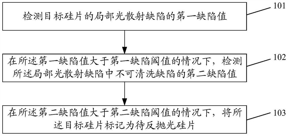
[0033]Such asfigure 1As shown, in one embodiment, the silicon wafer processing method includes the following steps:
[0034]Step 101: Detect the first defect parameter of the local light scattering defect of the target silicon wafer.
[0035]The local light scattering defects in this embodiment can be obtained by detecting the light scattering on the surface of the target silicon chip. It
PUM
 Abstract
Description
Claims
Application Information
 - R&D Engineer
- R&D Manager
- IP Professional
- Industry Leading Data Capabilities
- Powerful AI technology
- Patent DNA Extraction
Browse by: Latest US Patents, China's latest patents, Technical Efficacy Thesaurus, Application Domain, Technology Topic.
© 2024 PatSnap. All rights reserved.Legal|Privacy policy|Modern Slavery Act Transparency Statement|Sitemap