Preparation method of multi-layer glass substrate, glass substrate and Mini-LED glass substrate
A multi-layer glass, glass substrate technology, applied in the direction of multi-layer circuit manufacturing, printed circuit manufacturing, electrical components, etc., can solve the problem of easy short circuit, resin insulating layer can not effectively isolate the inner layer and outer circuit charge transmission, ion bombardment problems of depth
- Summary
- Abstract
- Description
- Claims
- Application Information
AI Technical Summary
Problems solved by technology
Method used
Image

Examples
Embodiment 1
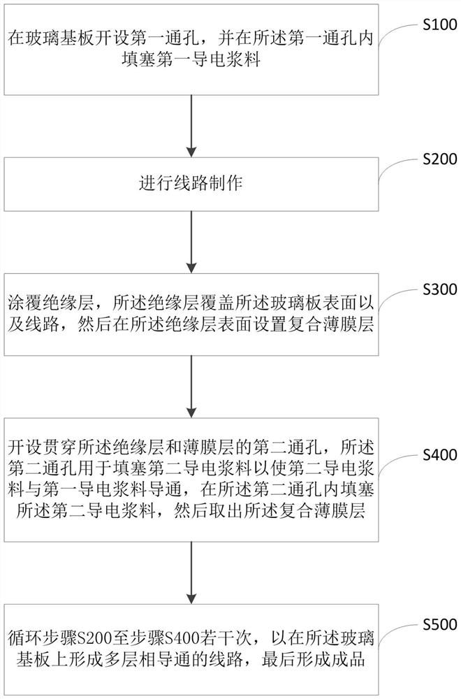
[0036] figure 1 It is a flow chart of a method for preparing a multilayer glass substrate provided according to an exemplary embodiment, such as figure 1 As shown, the method includes the following steps:
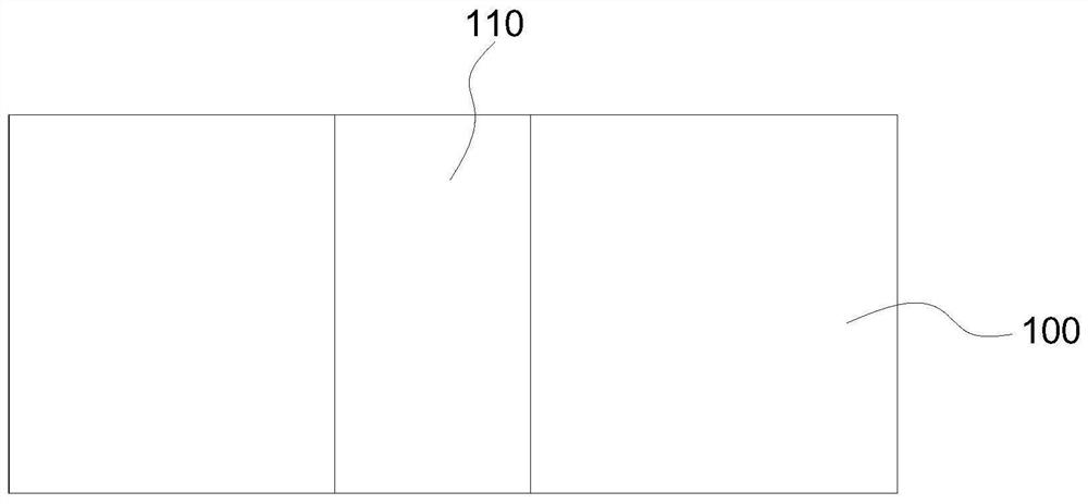
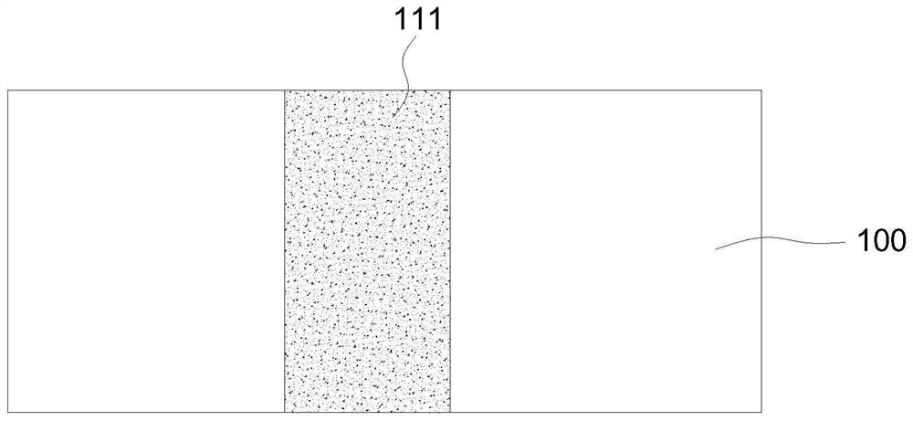
[0037] Step S100, please refer to figure 2 , the first through hole 110 is opened on the glass substrate 100, specifically, the first through hole 110 can be opened on the glass substrate 100 through a laser drilling process, and the laser drilling process can be carried out in a UV manner, please refer to image 3 , and fill the first through hole 110 with the first conductive paste 111. The conductive paste is a conductive paste, also known as interconnection paste, conductive copper paste or interconnection copper paste. The conductive paste can be screen printed or Apply it to the required parts of the substrate by other methods, and then sinter it at a specific temperature to form a conductor. It is mainly used for wiring of thick film integrated circuits, electrodes s
Embodiment 2
[0044] Both the first conductive paste 111 and the second conductive paste 311 contain: 30-50% copper powder, 20-40% tin powder, 0-3% silver powder, 5-10% bismuth powder, 0-10% % epoxy resin, 0-5% organic acid activator and 0.5-5% additives. This component system forms a low-temperature alloy type copper alloy. The metal powder is designed by alloying, and then combined with organic additives agent, etc. to achieve low-temperature sintering, and to ensure the formation of good IMC welding intergranular compounds, and can achieve sintering below 190°C, that is, the sintering temperature of the first conductive paste 111 and the second conductive paste 311 is less than 200°C, The energy consumption required for production is reduced, and at the same time, other components of the glass substrate are prevented from being damaged when the sintering temperature is too high, for example, higher than 400°C.
[0045] Further, the pore diameter of the first through hole 110 is 30-100 μm. F
Embodiment 3
[0047] The present disclosure also provides a glass substrate, which is made by any one of the methods for preparing a multi-layer glass substrate described above, wherein, please refer to Figure 10 , a glass substrate comprising: a glass substrate 100, the glass substrate 100 is provided with several first through holes 110, the first through holes 110 are filled with a first conductive paste 111, and the surface of the glass substrate 100 is provided with several layers in turn A circuit layer composed of a line 200 and an insulating layer 300, the insulating layer 300 is provided with a second through hole 310, and a second conductive paste 311 is arranged in the second through hole 310, and the second conductive paste 311 and the first conductive paste 111 is turned on.
PUM
| Property | Measurement | Unit |
|---|---|---|
| Aperture | aaaaa | aaaaa |
Abstract
Description
Claims
Application Information
 - R&D Engineer
- R&D Manager
- IP Professional
- Industry Leading Data Capabilities
- Powerful AI technology
- Patent DNA Extraction
Browse by: Latest US Patents, China's latest patents, Technical Efficacy Thesaurus, Application Domain, Technology Topic.
© 2024 PatSnap. All rights reserved.Legal|Privacy policy|Modern Slavery Act Transparency Statement|Sitemap