Planar PiN-type beta irradiation battery with passivation layer surface field and preparation method of planar PiN-type beta irradiation battery
A passivation layer and surface field technology, applied in the field of microelectronics, can solve the problems of increasing the saturation current of PiN devices, enhancing the negative impact of surface recombination, and limiting energy conversion efficiency, so as to reduce the saturation current, weaken the surface recombination, and improve The effect of energy conversion efficiency
- Summary
- Abstract
- Description
- Claims
- Application Information
AI Technical Summary
Benefits of technology
Problems solved by technology
Method used
Image

Examples
Embodiment 1
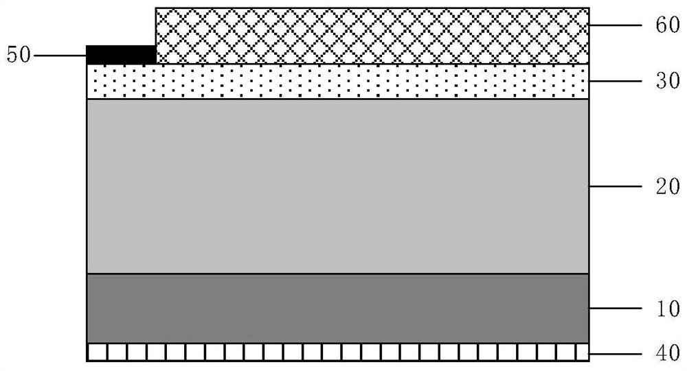
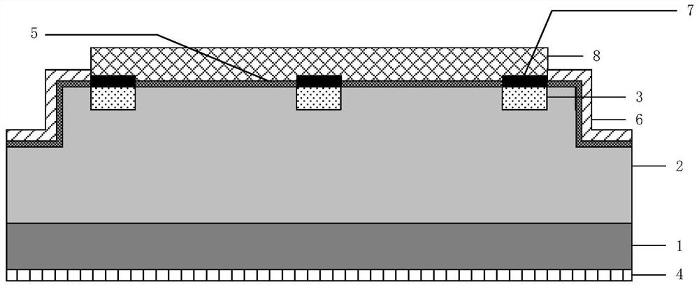
[0041] See figure 2 , figure 2A schematic structural diagram of a planar PiN-type β-irradiated cell with a passivation layer surface field provided by an embodiment of the present invention. The PiN unit and the radioisotope unit located on the PiN unit.
[0042] The PiN unit includes an N-type doped 4H-SiC substrate 1, an N-type doped 4H-SiC epitaxial layer 2, a P-type ion implantation region 3, an N-type ohmic contact electrode 4, a first passivation layer 5, and a second passivation layer. layer 6 and a P-type ohmic contact electrode 7 .
[0043] Specifically, the shape of the PiN unit includes but not limited to square or circle. When the PiN unit is square, its mesa area is 0.5×0.5cm~1.0×1.0cm; when the PiN unit is circular, its mesa area is Φ0.5cm~Φ1.0cm; the area of PiN unit is not limited to the above-mentioned area and size.
[0044] The N-type ohmic contact electrode 4, the N-type doped 4H-SiC substrate 1 and the N-type doped 4H-SiC epitaxial layer 2 are stacke
Embodiment 2
[0062] On the basis of Example 1, please refer to Figure 5a-Figure 5j , Figure 5a-Figure 5j A process schematic diagram of a method for preparing a planar PiN-type β-irradiated battery with a surface field of a passivation layer provided by an embodiment of the present invention, the preparation method includes steps:
[0063] S1. Epitaxial growth of N-type doped 4H-SiC epitaxial layer 2 on N-type doped 4H-SiC substrate 1, see Figure 5a with Figure 5b .
[0064]First, the N-type doped 4H-SiC substrate 1 sample is cleaned to remove surface pollutants.
[0065] Then, use chemical vapor deposition CVD to epitaxially grow a layer with a doping concentration of 1×10 on the cleaned N-type highly doped 4H-SiC substrate 1 sample surface. 14 ~1×10 15 cm -3 N-type low-doped 4H-SiC with a thickness of 4.0-10.0 μm forms an N-type doped 4H-SiC epitaxial layer 2 .
[0066] S2. Perform mesa etching on the N-type doped 4H-SiC epitaxial layer 2 to form an isolation mesa, see Figure 5
Embodiment 3
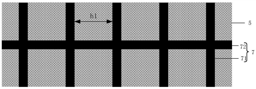
[0084] On the basis of Example 2, please combine Figure 5a-Figure 5j , this embodiment takes the preparation of a planar silicon carbide PiN-type β-irradiated cell with a grid-like distributed P-type region and a passivation layer surface field as an example to illustrate its preparation method, wherein the cell area is 0.7cm×0.7cm, P The pitch of the type injection regions is 300 μm, the number of electrodes in the vertical rectangular strip 71 is 22, and the number of electrodes in the horizontal rectangular strip 72 is 1.
[0085] S1. Epitaxial growth of an N-type doped 4H-SiC epitaxial layer 2 on an N-type doped 4H-SiC substrate 1 .
[0086] First, use standard RAC to clean the N-type doped 4H-SiC substrate 1 sample to remove surface pollutants, see Figure 5a .
[0087] Specifically, first at 25°C, the doping concentration is 5×10 18 cm -3 , a sample of N-type highly doped 4H-SiC substrate with a thickness of 380 μm was placed in H 2 SO 4 :H 2 o 2 Soak in the reagen
PUM
| Property | Measurement | Unit |
|---|---|---|
| Doping concentration | aaaaa | aaaaa |
| Thickness | aaaaa | aaaaa |
| Thickness | aaaaa | aaaaa |
Abstract
Description
Claims
Application Information
 - R&D Engineer
- R&D Manager
- IP Professional
- Industry Leading Data Capabilities
- Powerful AI technology
- Patent DNA Extraction
Browse by: Latest US Patents, China's latest patents, Technical Efficacy Thesaurus, Application Domain, Technology Topic.
© 2024 PatSnap. All rights reserved.Legal|Privacy policy|Modern Slavery Act Transparency Statement|Sitemap