Integral accumulation storage circuit
A storage circuit and integration technology, applied in the field of integration accumulation storage circuit, can solve the problems of incompatibility of switching power supply control circuit production process, hinder the miniaturization development of switching power supply control circuit system, expensive digital integrator, etc., to avoid integration operation. Effects of overflow, increased input signal range, and low cost
- Summary
- Abstract
- Description
- Claims
- Application Information
AI Technical Summary
Benefits of technology
Problems solved by technology
Method used
Image

Examples
Embodiment 1
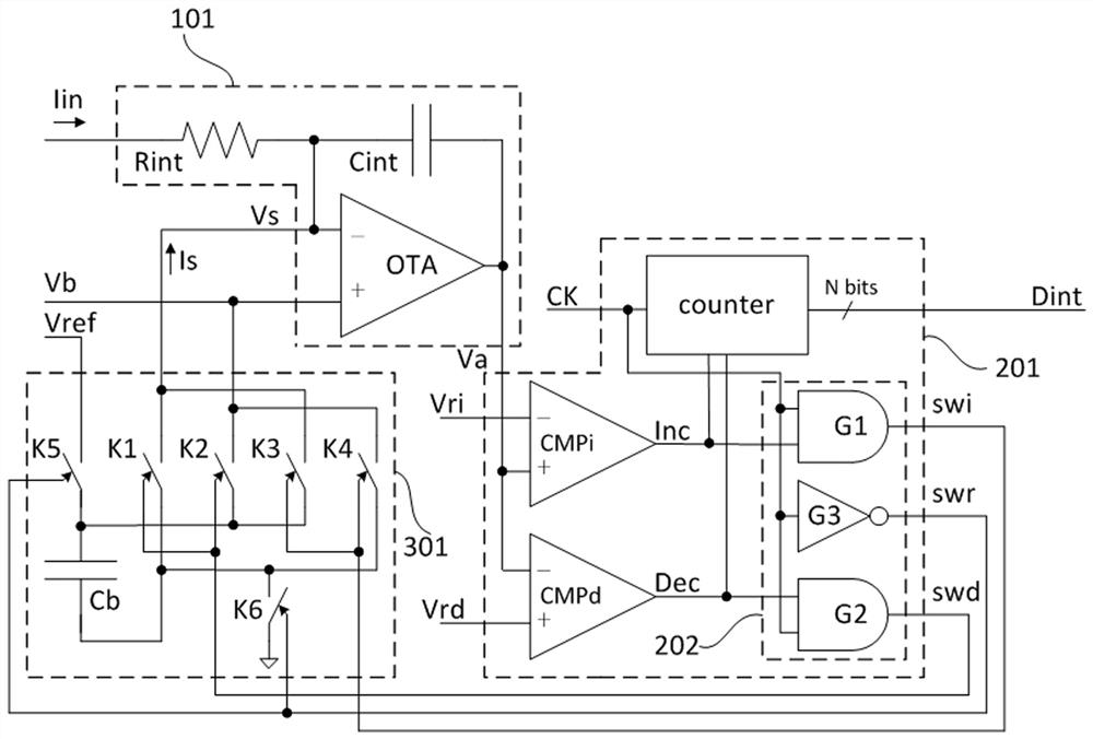
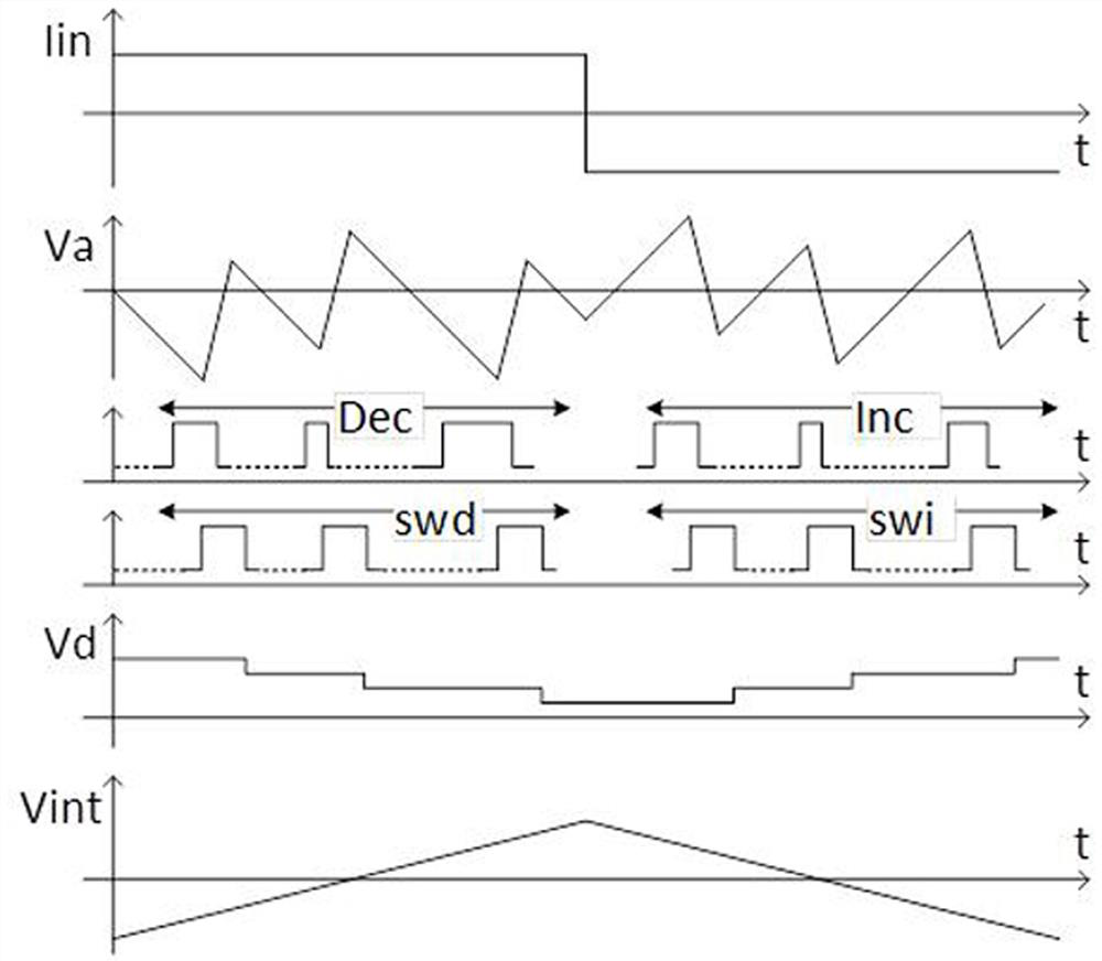
[0052] Such as figure 1 As shown, an integral accumulation storage circuit, which receives the compensation current Iin, generates an adjustment voltage Va in the form of an analog voltage, outputs an accumulation value Dint in the form of a digital signal with a bit width of N bits, the amplitude of the adjustment voltage Va and the accumulation value Dint The value of the value Dint is determined by the integral value of the compensation current Iin with respect to time.
[0053] Specifically, the integration and accumulation storage circuit includes an integration module 101, a decomposition and accumulation module 201, and a charge balance module 301, and the integration module 101 is used to simultaneously perform integral operations on the compensation current Iin and the balance current Is to generate For the adjustment voltage Va, the decomposing and accumulating module 201 is used to decompose the accumulated charge in the integral operation into quantization units of fi
Embodiment 2
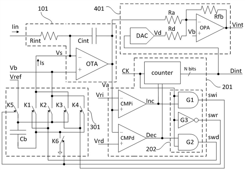
[0077] The difference from the previous examples is that, if image 3As shown, the integral accumulation storage circuit also includes an error elimination module 401, the first input terminal of the error elimination module 401 is connected to the first output terminal of the decomposition and accumulation module 201, and receives the accumulated value Dint, and the second The input terminal is connected to the output terminal of the integrating module 101 to receive the regulated voltage Va, and the output terminal outputs the integrated voltage Vint. The error elimination module 401 comprises a digital-to-analog converter DAC, an operational amplifier OPA, a value input resistance Rd, an adjustment input resistance Ra and a feedback resistance Rfb; The first input end) receives the accumulated value Dint, and the output end outputs the accumulated value voltage Vd in the form of an analog signal; one end of the value input resistor Rd receives the accumulated value voltage Vd,
PUM
 Abstract
Description
Claims
Application Information
 - R&D Engineer
- R&D Manager
- IP Professional
- Industry Leading Data Capabilities
- Powerful AI technology
- Patent DNA Extraction
Browse by: Latest US Patents, China's latest patents, Technical Efficacy Thesaurus, Application Domain, Technology Topic.
© 2024 PatSnap. All rights reserved.Legal|Privacy policy|Modern Slavery Act Transparency Statement|Sitemap