Photomask manufacturing method, photomask, photoetching method, medium, module and photoetching machine
A photomask and photolithography technology, which is applied in the field of microelectronics, can solve problems such as poor surface flatness of wafers or workpieces, pattern defocus, transfer accuracy of feature patterns, and reduced yield.
- Summary
- Abstract
- Description
- Claims
- Application Information
AI Technical Summary
Problems solved by technology
Method used
Image

Examples
Embodiment Construction
[0070] The present invention will be further described in detail below in conjunction with the accompanying drawings and embodiments. Of course, the specific embodiments described below are only for explaining the technical solution of the present invention, rather than limiting the present invention.
[0071] In addition, the parts described in the embodiments or the drawings are only illustrations of relevant parts of the present invention, rather than the entirety of the present invention.
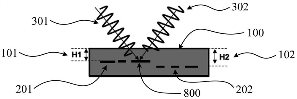
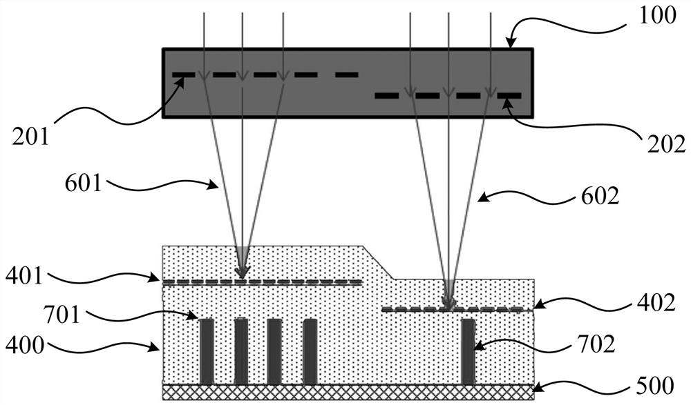
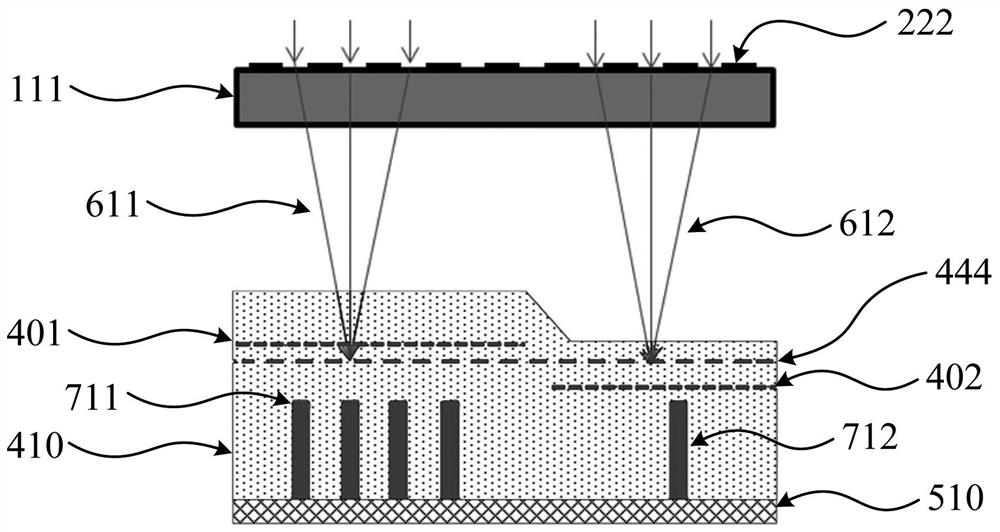
[0072] Such as figure 2 As shown, in order to solve the technical problem of photolithography defocusing, the embodiment of the present invention discloses a method for making a mask that can match the surface topography of a wafer or workpiece; by detecting the surface of the workpiece, the surface topography is represented in layers , and then achieve matching with the above-mentioned surface topography through a multi-layer photomask.
[0073] Specifically, such as figure 2 , quant
PUM
 Abstract
Description
Claims
Application Information
 - R&D Engineer
- R&D Manager
- IP Professional
- Industry Leading Data Capabilities
- Powerful AI technology
- Patent DNA Extraction
Browse by: Latest US Patents, China's latest patents, Technical Efficacy Thesaurus, Application Domain, Technology Topic.
© 2024 PatSnap. All rights reserved.Legal|Privacy policy|Modern Slavery Act Transparency Statement|Sitemap