On-chip cache design method with memory stack compilation and layout collaboration and on-chip cache
An on-chip cache and design method technology, applied in static memory, computer-aided design, CAD circuit design, etc., can solve problems such as large timing margin, and achieve the effects of power consumption optimization, power consumption improvement, and area reduction
- Summary
- Abstract
- Description
- Claims
- Application Information
AI Technical Summary
Benefits of technology
Problems solved by technology
Method used
Image

Examples
Embodiment Construction
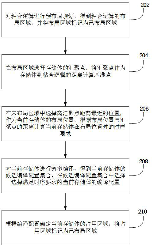
[0052] In order to make the purpose, technical solution and advantages of the present application clearer, the present application will be further described in detail below in conjunction with the accompanying drawings and embodiments. It should be understood that the specific embodiments described here are only used to explain the present application, and are not intended to limit the present application.
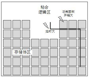
[0053] The traditional layout structure of on-chip cache is as follows figure 1 As shown, the main body is a storage array composed of memory banks, and the outside of the storage array is glue logic, including a series of merging, selection, registration operations or bus protocol conversion logic, and finally output to the external unit or bus. Specifically, the memory bank may be an SRAM memory bank. Due to the large size of the memory banks, the distance of the memory banks from the glue logic varies in different locations. Such as figure 1 The memory bank in the middl
PUM
 Abstract
Description
Claims
Application Information
 - R&D Engineer
- R&D Manager
- IP Professional
- Industry Leading Data Capabilities
- Powerful AI technology
- Patent DNA Extraction
Browse by: Latest US Patents, China's latest patents, Technical Efficacy Thesaurus, Application Domain, Technology Topic.
© 2024 PatSnap. All rights reserved.Legal|Privacy policy|Modern Slavery Act Transparency Statement|Sitemap