Semiconductor packaging fixing device

A fixing device and semiconductor technology, which is applied in semiconductor/solid-state device manufacturing, electrical components, circuits, etc., can solve the problems of poor fixing effect and easy deformation of fixing devices, so as to improve the pressing effect, avoid the pressure plate from hurting the line arc, and ensure The effect of accuracy

Pending Publication Date: 2022-05-31
ZHUHAI GREE XINYUAN ELECTRONICS +1
View PDF0 Cites 0 Cited by
  • Summary
  • Abstract
  • Description
  • Claims
  • Application Information

AI Technical Summary

Benefits of technology

The present in this patented technology describes an improved way for sealing electronic components during manufacturing processes with epoxy resin capsules. This improves stability over time without causing damage or affecting performance due to pressure applied through manual supports used to hold them tight together. It also enhances the precision of measurements made from these materials compared against previous methods while maintaining their strength properties.

Problems solved by technology

This patented technical problem addressed in this patents relating to testing electronic components during manufacturing involves ensuring stable fixation for chips while also minimizing any negative side effects such as tilting off other parts when carrying out tests with different tools used for bonding purposes.

Method used


Image

  • Semiconductor packaging fixing device
  • Semiconductor packaging fixing device
  • Semiconductor packaging fixing device

Examples


Embodiment Construction

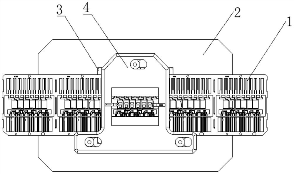
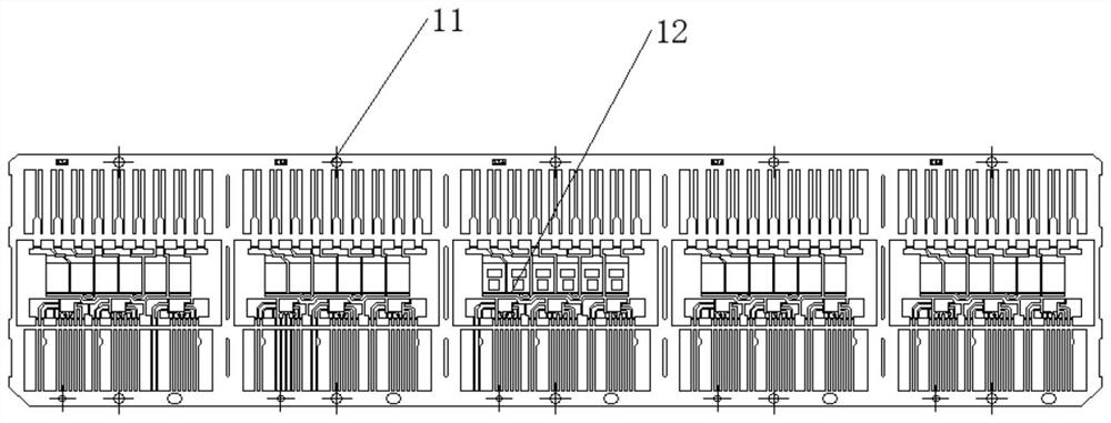
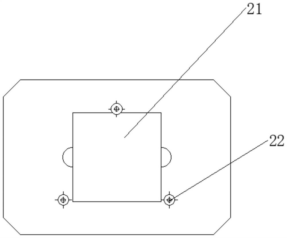
[0031] The following is a detailed description of a semiconductor package fixing device provided by the present invention as shown in FIG. 1 to FIG. 6 .

[0038] Further, one side of the through groove is provided with a bump 31, and the shape and quantity of the bump 31 are not specifically limited here.

[0041] As a preferred embodiment, the fixing structure is at least one fixing post 22, and the matching portion includes at least one fixing hole,

[0043] Further, the base 2 is provided with a fixed groove 21, and the cushion block 3 is accommodated in the fixed groove 21 to limit the movement of the cushion block 3.

[0045] Further, the pressing plate 4 is provided with a pressing claw 43, and the pressing claw 43 presses down and contacts the bracket 1 so that the bracket 1 and the pad 3 are fixed,


PUM


Abstract

The invention discloses a semiconductor packaging fixing device which comprises a base and a support, a cushion block is arranged on the base, a pressing plate is arranged on the support, and the pressing plate and the base are fixed so that the support and the cushion block can be fixedly connected. According to the semiconductor packaging fixing device provided by the invention, the cushion block and the pressing plate are designed, and a plurality of fixing structures are arranged on the cushion block and the pressing plate, so that the bracket is more firmly fixed, the phenomenon that a wire arc is crushed by the pressing plate due to improper manual placement of the bracket is avoided, the pressing effect of the bracket in the push-pull force process is improved, and the data accuracy is ensured.

Description


Claims


Application Information

Patent Timeline
Owner ZHUHAI GREE XINYUAN ELECTRONICS
Why Eureka
Try Eureka