Display panel and display device
- Summary
- Abstract
- Description
- Claims
- Application Information
AI Technical Summary
Benefits of technology
Problems solved by technology
Method used
Image


Examples
Example
Embodiment 1
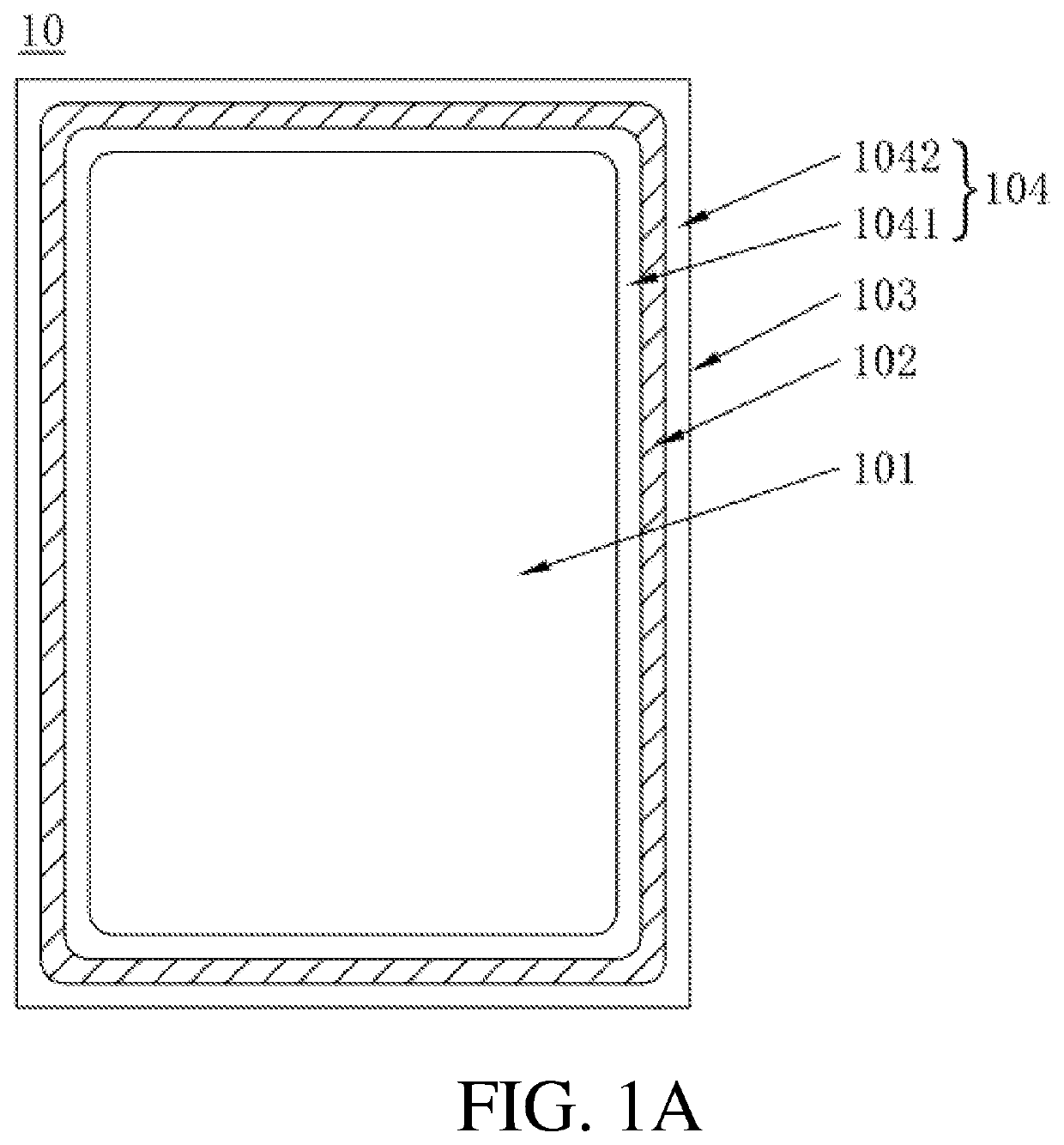
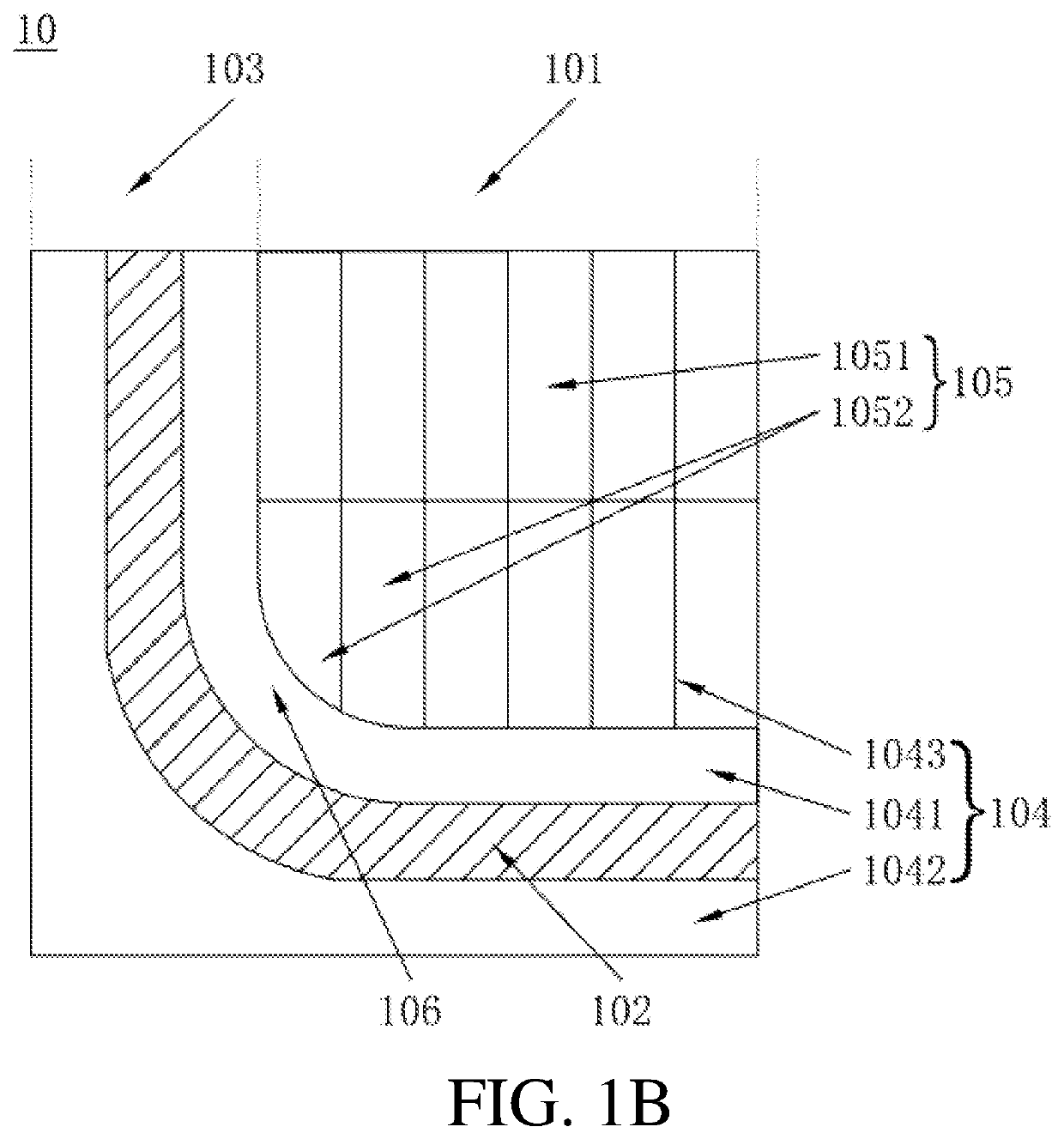
[0062]As shown in FIG. 2, the first substrate 20 includes a display area 201 and a bezel area 203, and the bezel area 203 is provided with a sealant 202 surrounding the display area 201.
[0063]The black matrix 204 is further disposed on the first substrate 20, and the black matrix 204 includes first black matrices 2041 and 2042 positioned in the bezel area 203 and a second black matrix 2043 disposed in the display area 201, wherein the first black matrices 2041 and 2042 include an inner bezel 2041 between the display area 201 and the sealant 202 and an outer bezel 2042 positioned on a side of the sealant 202 away from the display area 201.
[0064]The inner bezel 2041 is provided with the widened portion 206 at the corner, and a position of the inner bezel 2041 provided with the widened portion 206 is arced.
[0065]In addition, the second black matrix 2043 separates the display area 201 into a plurality of sub-pixel 205, including irregularly shaped sub-pixels 2052 within the dis
Example
Embodiment 2
[0073]As shown in FIG. 3, the first substrate 30 includes a display area 301 and a bezel area 303, and the bezel area 303 is provided with a sealant 302 surrounding the display area 301.
[0074]The black matrix 304 is further disposed on the first substrate 30, and the black matrix 304 includes first black matrices 3041 and 3042 positioned in the bezel area 303, and a second black matrix 3043 disposed in the display area 301, wherein the first black matrices 3041 and 3042 include an inner bezel 3041 between the display area 301 and the sealant 302 and an outer bezel 3042 positioned on a side of the sealant 302 away from the display area 301.
[0075]The inner bezel 3041 is provided with the widened portion 306 at the corner, and a position of the inner bezel 3041 provided with the widened portion 306 is arced.
[0076]In addition, the second black matrix 3043 separates the display area 301 into a plurality of sub-pixel 305, including irregularly shaped sub-pixels 3052 within the di
Example
Embodiment 3
[0084]As shown in FIG. 4, the first substrate 40 includes a display area 401 and a bezel area 403, and the bezel area 403 is provided with a sealant 402 surrounding the display area 401.
[0085]The black matrix 404 is further disposed on the first substrate 40, and the black matrix 404 includes first black matrices 4041 and 4042 positioned in the bezel area 403, and a second black matrix 4043 disposed in the display area 401, wherein the first black matrices 4041 and 4042 include an inner bezel 4041 between the display area 401 and the sealant 402 and an outer bezel 4042 positioned on a side of the sealant 402 away from the display area 401.
[0086]The inner bezel 4041 is provided with the widened portion 406 at the corner, and a position of the inner bezel 4041 provided with the widened portion 406 is arced.
[0087]In addition, the second black matrix 4043 separates the display area 401 into a plurality of sub-pixel 405, including irregularly shaped sub-pixels 4052 within the di
PUM
 Abstract
Description
Claims
Application Information
 - R&D Engineer
- R&D Manager
- IP Professional
- Industry Leading Data Capabilities
- Powerful AI technology
- Patent DNA Extraction
Browse by: Latest US Patents, China's latest patents, Technical Efficacy Thesaurus, Application Domain, Technology Topic.
© 2024 PatSnap. All rights reserved.Legal|Privacy policy|Modern Slavery Act Transparency Statement|Sitemap