Conductive particle and adhesive agent
a technology of adhesive agent and conductive particle, which is applied in the direction of non-conductive materials with dispersed conductive materials, natural mineral layered products, synthetic resin layered products, etc., can solve the problems of lowering the conductive reliability of the electric device b>101/, and it is difficult to use conductive particles of the same kind for connection between various kinds of adherends, etc., to achieve reliable electrical connection
- Summary
- Abstract
- Description
- Claims
- Application Information
AI Technical Summary
Benefits of technology
Problems solved by technology
Method used
Image

Examples
example 1
PRACTICE EXAMPLE 1
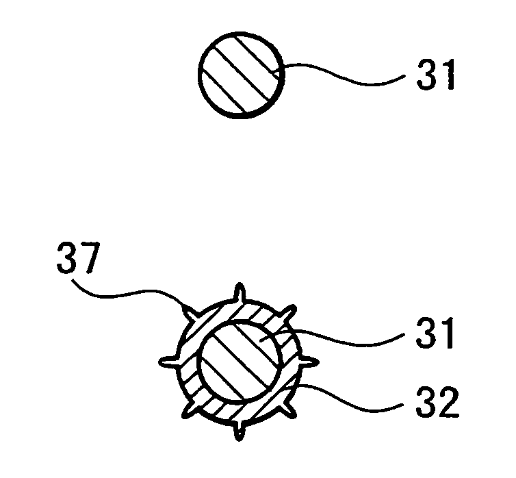
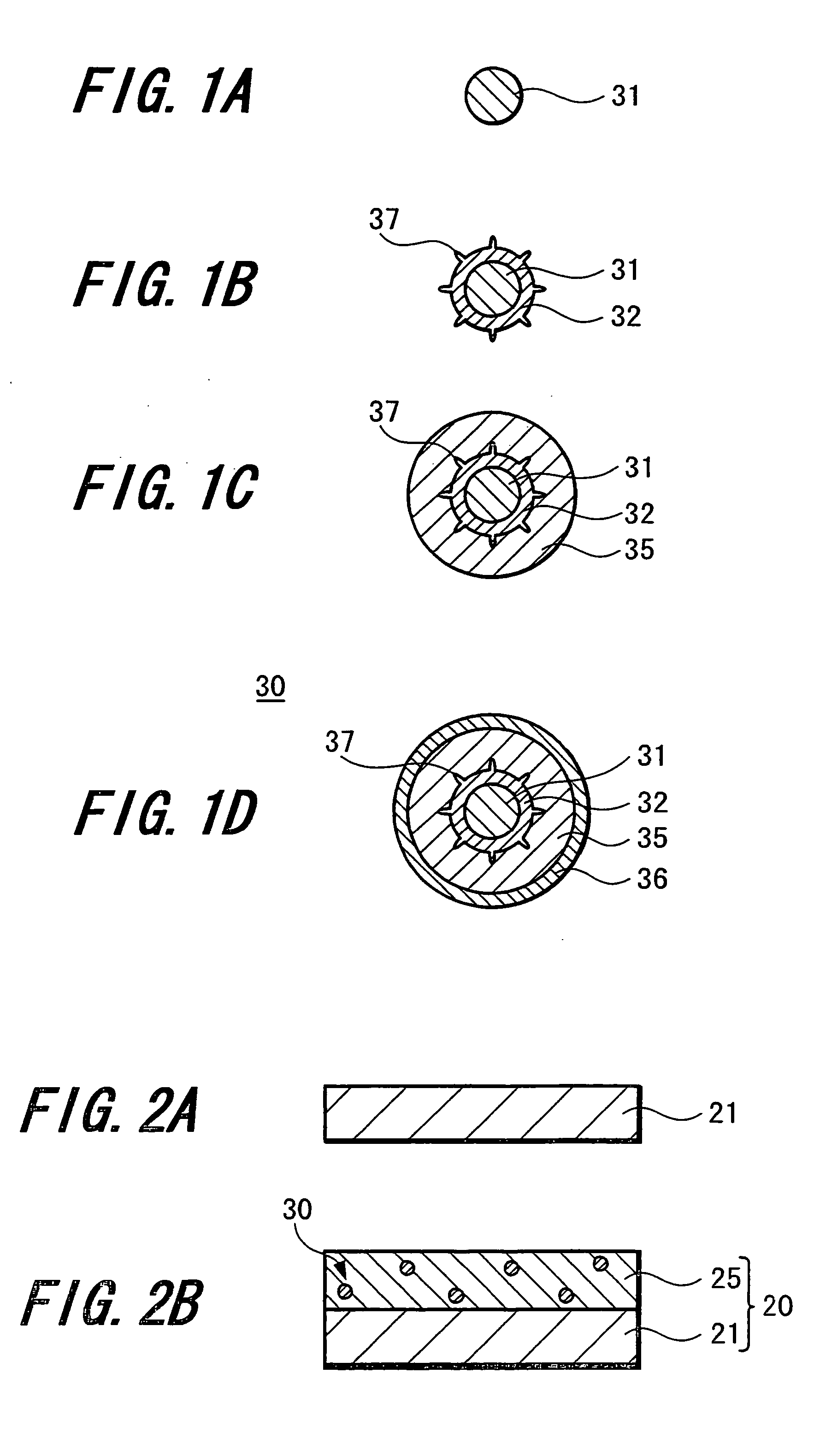
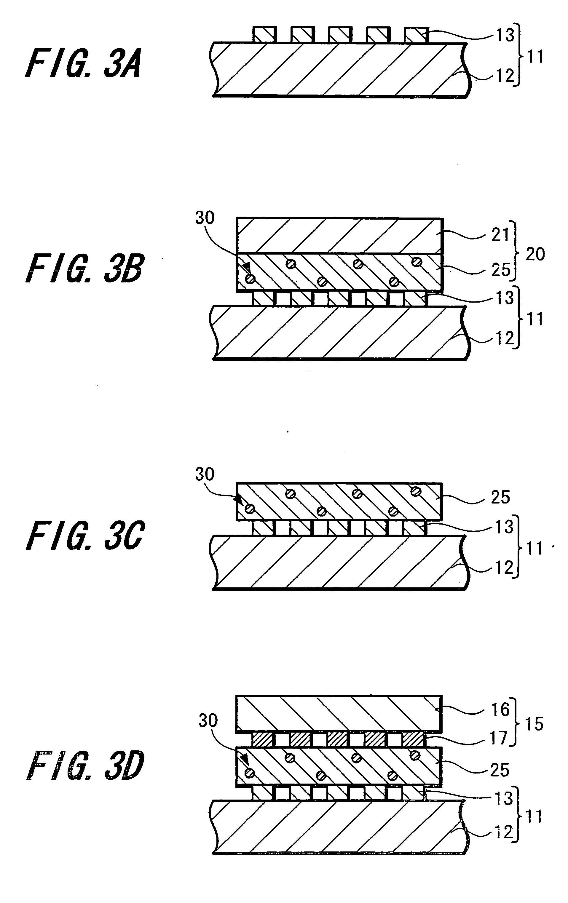
[0103] In this practice example the above-mentioned conductive particle 30 was produced.
[0104] In this case, first of all, a resin particle 31 of 2 μm in diameter was produced using a resin made of a divinylbenzene polymer whose K value is 600 kgf / mm2 and breaking strength 3.2 gf at the time when pressed and deforms by 10%. Next, after a nickel coating of 0.15 μm in thickness was formed on the surface of the resin particle 31 by means of plating, a gold coating of 0.02 μm in thickness was formed on the surface of the nickel coating by means of plating, and a first conductive thin film 32 composed of the nickel coating and the gold thin film was formed. There were no convex portions formed on the surface of the first conductive thin film 32.
[0105] Then, a powdery resin material made of an acrylic resin, whose K value by 10% is 300 kgf / mm2 and breaking strength 1.3 gf at the time when pressed and deforms, was used; this resin material, and the resin particle 31 on
example 2
PRACTICE EXAMPLE 2
[0107] In this practice example the aforementioned conductive particle 40 was produced.
[0108] In this case, first, a conductive particle 30 was produced by a similar method to the practice example 1. Then, a second resin coating 39 of 0.1 μm in thickness made of acrylic styrene resin is formed on the surface of a second conductive thin film 36 of the conductive particle 30 to obtain a conductive particle 40.
[0109] As regards each of the above-mentioned conductive particles 30 and 40 of practice examples 1 and 2: when the total weight of the first and second conductive thin films 32 and 36 is divided by the whole weight of each of the conductive particles 30 and 40 and then is multiplied by 100 each to calculate the metal content by percentage (metallization rate) of each of the conductive particles 30 and 40 of practice examples 1 and 2, each metallization rate was 50%.
example 3
PRACTICE EXAMPLE 3
[0110] In this practice example, a conductive particle 30 was produced by means of a similar method to the practice example 1; however, in this practice example 3, the first conductive thin film 32 was composed of a nickel coating of 0.01 μm in thickness and a gold coating of 0.01 μm in thickness.
PUM
| Property | Measurement | Unit |
|---|---|---|
| Fraction | aaaaa | aaaaa |
| Thickness | aaaaa | aaaaa |
| Thickness | aaaaa | aaaaa |
Abstract
Description
Claims
Application Information
 - R&D Engineer
- R&D Manager
- IP Professional
- Industry Leading Data Capabilities
- Powerful AI technology
- Patent DNA Extraction
Browse by: Latest US Patents, China's latest patents, Technical Efficacy Thesaurus, Application Domain, Technology Topic.
© 2024 PatSnap. All rights reserved.Legal|Privacy policy|Modern Slavery Act Transparency Statement|Sitemap