OLED active matrix cell designed for optimal uniformity

a technology of active matrix and cell, applied in the direction of instruments, static indicating devices, etc., can solve the problems of limiting the number of available gray levels, affecting the image quality, and affecting the uniformity of the active matrix,

Inactive Publication Date: 2007-10-11
EMAGIN CORP
View PDF6 Cites 158 Cited by
  • Summary
  • Abstract
  • Description
  • Claims
  • Application Information

AI Technical Summary

Benefits of technology

This invention relates to an electronic device that uses light-emitting elements (OLE) for display purposes or other applications such as backlighting displays on LCD screens. It achieves this by connecting two transistors together with another type called a diodes made up of PMOS tranductor material. These devices are designed to prevent damage caused when there're any electrical connections being established through them during use.

Problems solved by technology

The patent text discusses various techniques and prior art related to overcoming threshold voltage variation in direct view AMOLED displays using non-crystalline silicon processes. The technical problems addressed in the text include the high threshold voltage variability, the need for threshold voltage compensation, limitations of existing designs, signal distortions, susceptibility to crosstalk, and the desire for high precision drive.

Method used


Image

  • OLED active matrix cell designed for optimal uniformity
  • OLED active matrix cell designed for optimal uniformity
  • OLED active matrix cell designed for optimal uniformity

Examples


Embodiment Construction

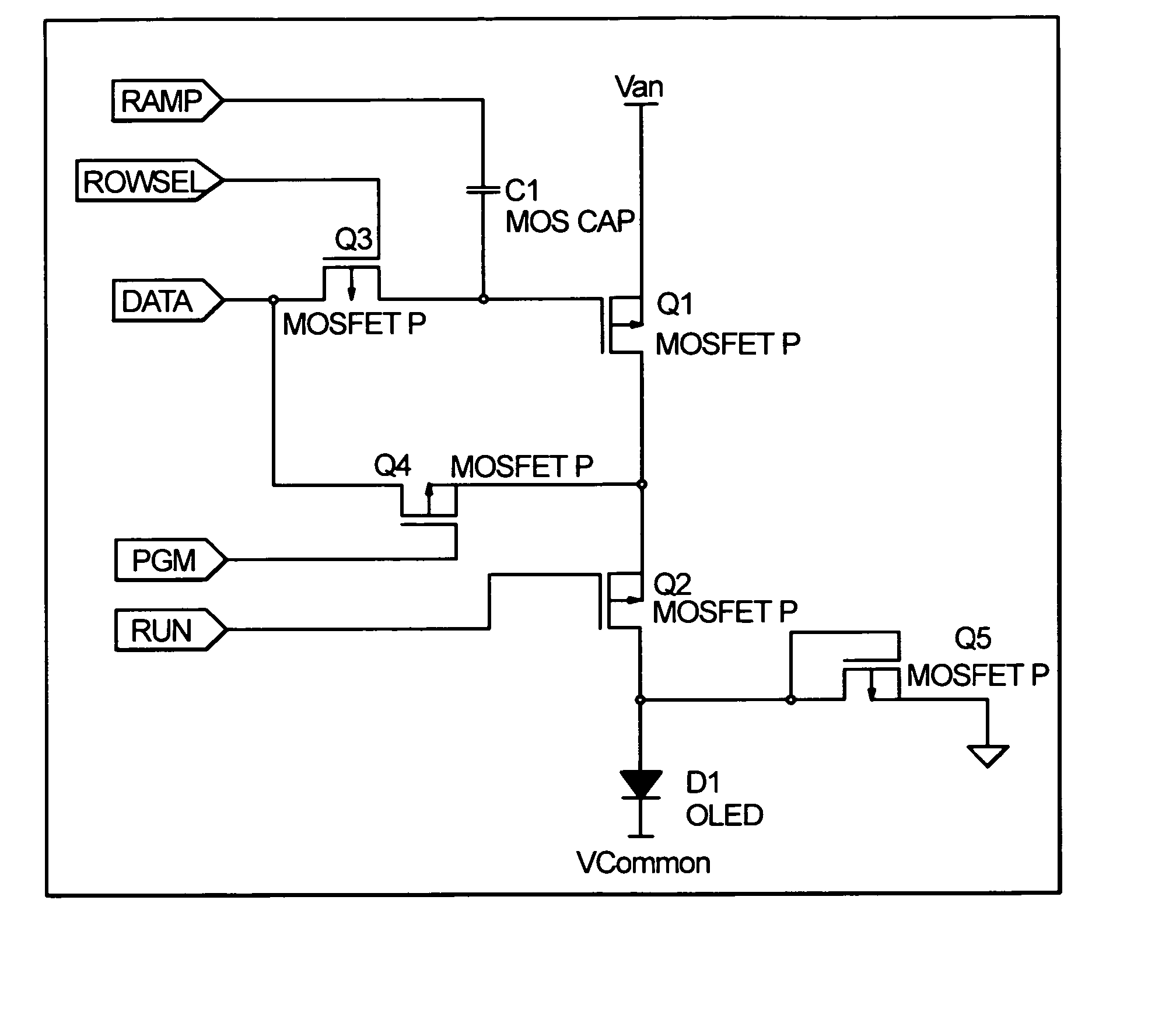
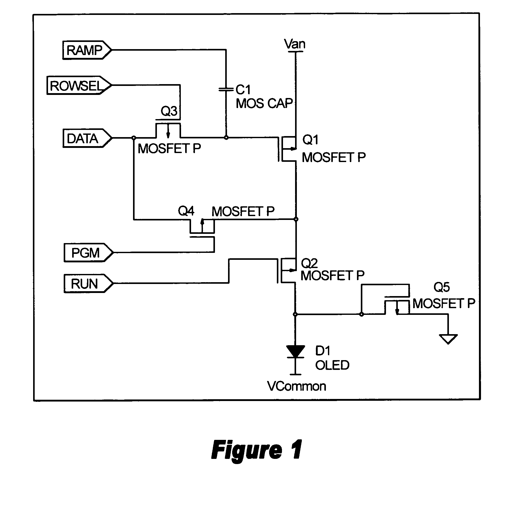
[0052]FIG. 1 shows a first preferred embodiment of the present invention in which the OLED pixel driver is a current source formed by a drive transistor Q1 and a storage capacitor C1. The voltage stored across capacitor C1 sets the current that flows through the output circuit of drive transistor Q1 and into OLED D1 (when the Run transistor Q2 is turned on). OLED D1 emits a light proportional to the current flowing through it.

[0053] Transistor Q5 is a diode configured PMOS transistor that protects the rest of the pixel driver from possible shorts across OLED D1.

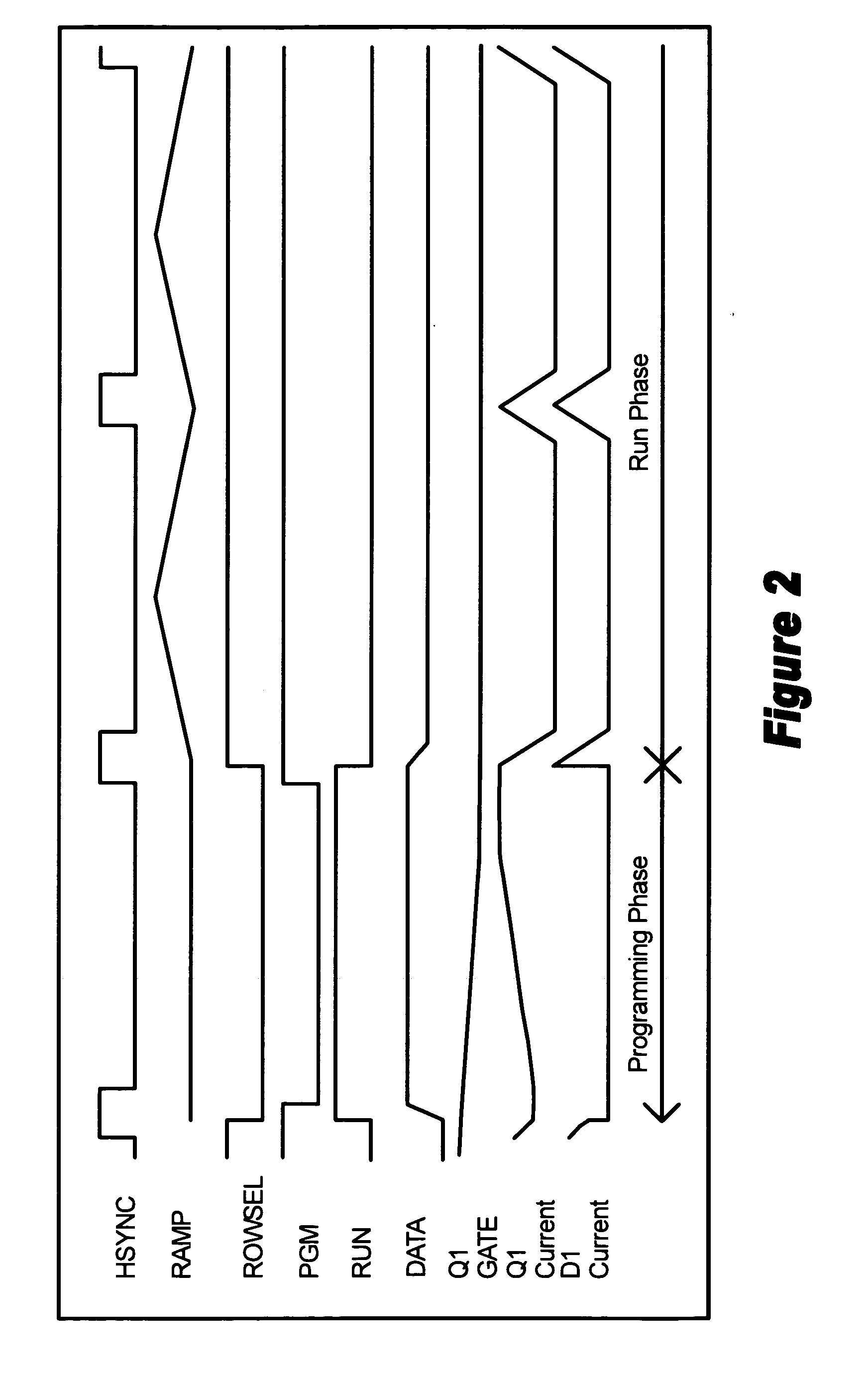
[0054] The Run transistor Q2 is turned off during the pixel driver programming phase. It is turned on during the Run phase to allow light emission.

[0055] Transistors Q3 and Q4 form a transmission gate means that is responsive to control signals to program the pixel driver with the source data information. The DATA terminal is connected to a current sink whose value represents the desired light (or gray) level. The combination


PUM


Abstract

A drive circuit is provided for an OLED pixel display. The drive circuit is adapted for use with a reference voltage source. It includes a first transistor and an OLED. The output circuit of the first transistor is operably connected between the reference voltage source and the OLED. Transmission gate means responsive to a control signal are provided to transmit a data signal to the first transistor. Means are provided for controlling the first transistor in accordance with a time domain modulation signal to provide an average current to the OLED which is a function of the data signal.

Description


Claims


Application Information

Patent Timeline
Owner EMAGIN CORP
Why Eureka
Try Eureka