Solid-state imaging apparatus

a technology of solid-state imaging and imaging apparatus, which is applied in the direction of color television details, television system details, television systems, etc., can solve problems such as image distortion

Inactive Publication Date: 2008-02-07
OLYMPUS CORP
View PDF8 Cites 39 Cited by
  • Summary
  • Abstract
  • Description
  • Claims
  • Application Information

AI Technical Summary

Benefits of technology

The present invention provides a solid state imaging device with multiple units arranged in rows and columns. Each unit has different parts like photosensitive elements and transistors. These components work together to capture images from different angles. A reset controller can be used to reset individual pixels before capturing another frame. After a certain amount of time, a reset controller activates the reset of one specific component while the other remains active. This allows for more accurate and reliable imaging results. Additionally, a special feature called a difference correction mechanism can be applied to improve the accuracy of the captured image.

Problems solved by technology

This patent describes a technique called "global shutter” technology for improving the performance of solid-state imaging devices. It involves driving multiple columns of pixels in sequence to capture images quickly. However, it also includes various technical features related to the use of specific elements like transistors and resistive switching circuits in the imaging process. These improvements help improve the speed and accuracy of the overall system.

Method used


Image

  • Solid-state imaging apparatus
  • Solid-state imaging apparatus
  • Solid-state imaging apparatus

Examples


first embodiment

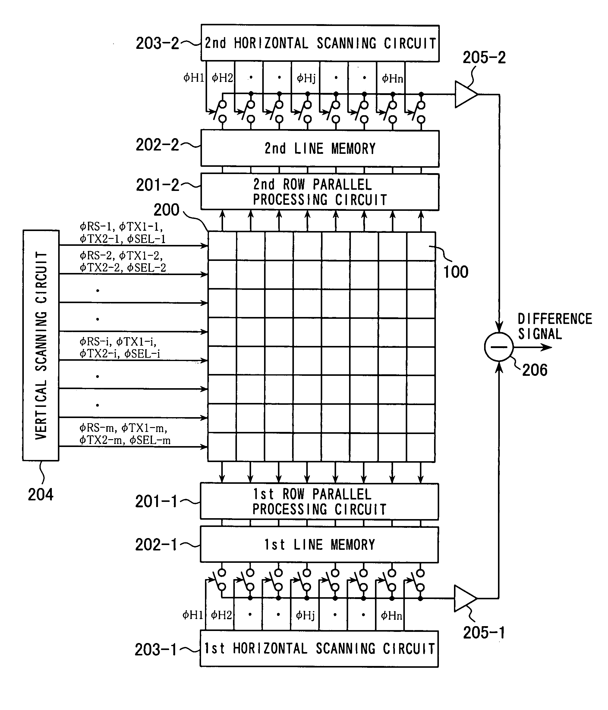
[0049]FIG. 9 is a block diagram showing construction of the solid-state imaging apparatus according to the invention. In FIG. 9, what is denoted by 1 is an imaging optical system for image taking of which focal distance and stop are controlled by an optical system control circuit 12. Denoted by 2 is a solid-state imaging device having an equivalent construction as that of the above described fundamental construction where each signal can be independently outputted of the first pixel and the second pixel constituting a unit pixel, disposed at locations that are regarded as substantially the same location at which image is formed by the imaging optical system 1. Drive of the solid-state imaging device is controlled by a drive circuit 8 so that similar operation as that shown in the above fundamental construction can also be effected. Denoted by 3, 4 each are an A / D conversion apparatus for converting output signal of the solid-state imaging device 2 into digital signal, which are conne

third embodiment

[0089]In this manner, with the solid-state imaging apparatus according to the above third embodiment, correction of shading also becomes possible in addition to correction of sensitivity characteristic difference between the signals of the first pixel and of the second pixel so that image taking data of even higher quality can be acquired. Also in the shading correction, high-quality image taking data can always be acquired even if the conditions such as focal length and stop of the imaging optical system are changed.

[0090]It is desirable that the correction data for the shading correction are also provided for each of the conditions of focal distance and stop of the imaging optical system and, if the taking lens is interchangeable, for each taking lens. However, it is not necessary to provide correction data for each of all conditions, and it is possible to substitute correction data under a certain condition for another or to make a desired correction data from correction data under


PUM


Abstract

A solid-state imaging apparatus including: a pixel section having two-dimensionally arrayed unit pixels each having a first pixel and a second pixel respectively containing photoelectric conversion devices that are located at positions regarded as the same position at which image is formed by an imaging optical system; a reset control means for simultaneously resetting respectively independently all first pixels and all second pixels of each unit pixel arrayed in the pixel section; a difference signal output means for obtaining a difference signal between signals of the first pixel and of the second pixel; a control section for rendering control such that a reset is effected of signals of all first pixels of the pixel section and, after a desired exposure time, a reset is effected of signals of all second pixels of the pixel section by the reset control means, and then signals of the first pixel and of the second pixel are read out respectively in a simultaneous or substantially simultaneous manner immediately after the reset of signal of all second pixels by the reset control means so as to output a difference signal between these as imaging signal by the difference signal output means; and a characteristic difference correction means for correcting a characteristic difference between the first pixel and the second pixel.

Description


Claims


Application Information

Patent Timeline
Owner OLYMPUS CORP
Why Eureka
Try Eureka