Image sensing apparatus and imaging system
- Summary
- Abstract
- Description
- Claims
- Application Information
AI Technical Summary
Benefits of technology
Problems solved by technology
Method used
Image

Examples
Example
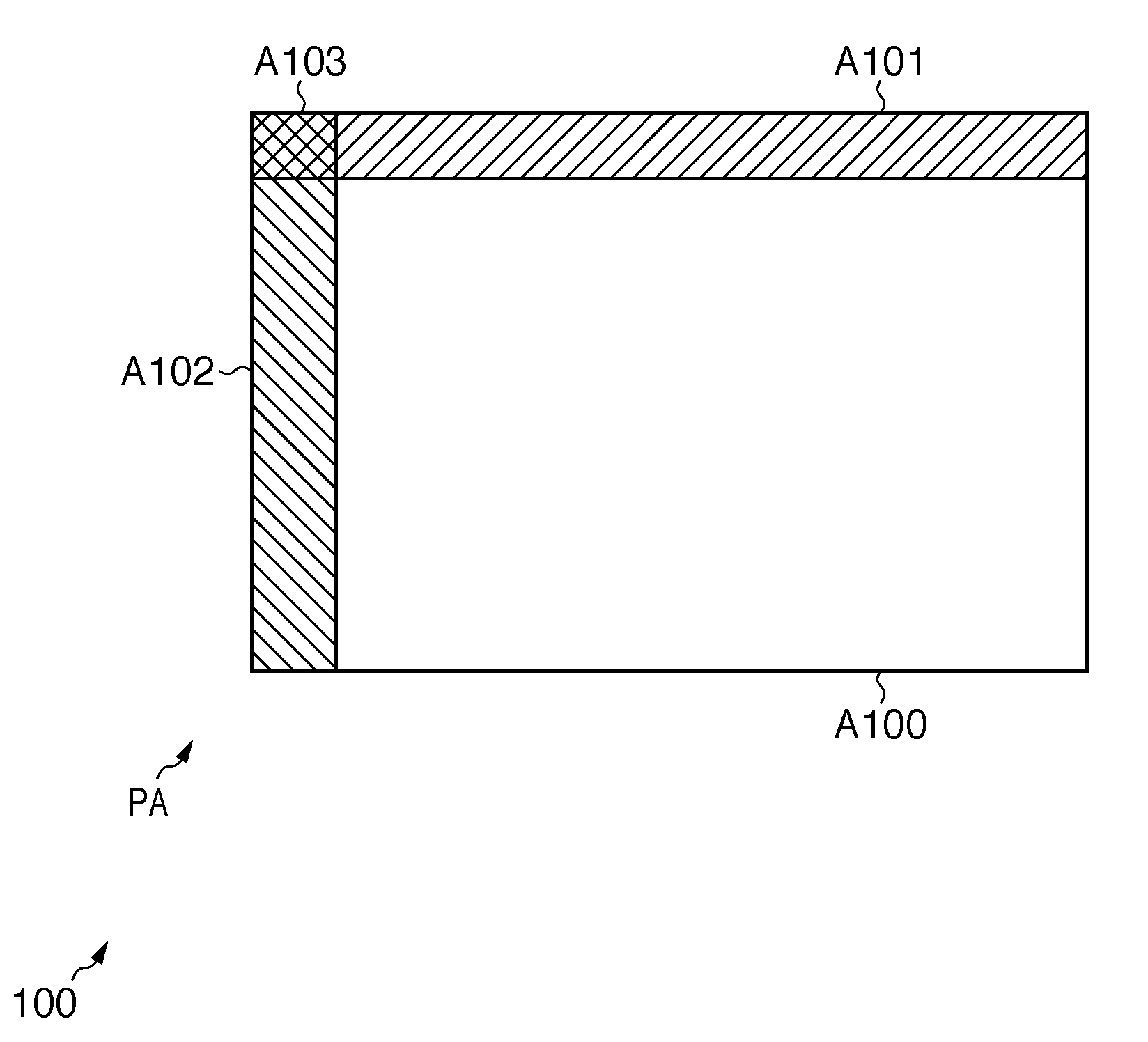
[0023]An image sensing apparatus 100 according to the first embodiment of the present invention will be described with reference to FIG. 1. FIG. 1 is a view showing the arrangement of the image sensing apparatus 100 according to the first embodiment of the present invention.
[0024]The image sensing apparatus 100 includes a pixel array PA and peripheral circuits (not shown).
[0025]In the pixel array PA, pixels are arrayed in the row and column directions (two-dimensionally). The pixel array PA includes optical black areas (light-shielded areas: to be referred to as OB areas hereinafter) A101 to A103, and an effective area A100. The OB areas A101 to A103 are arranged around the effective area A100 in the pixel array PA. The OB areas are shielded from light by a light-shielding film and / or wiring layer.
[0026]The OB areas A101 to A103 include the vertical OB area A101, horizontal OB area A102, and vertical & horizontal OB area A103. The vertical OB area A101 is arranged adjacent to an end
Example
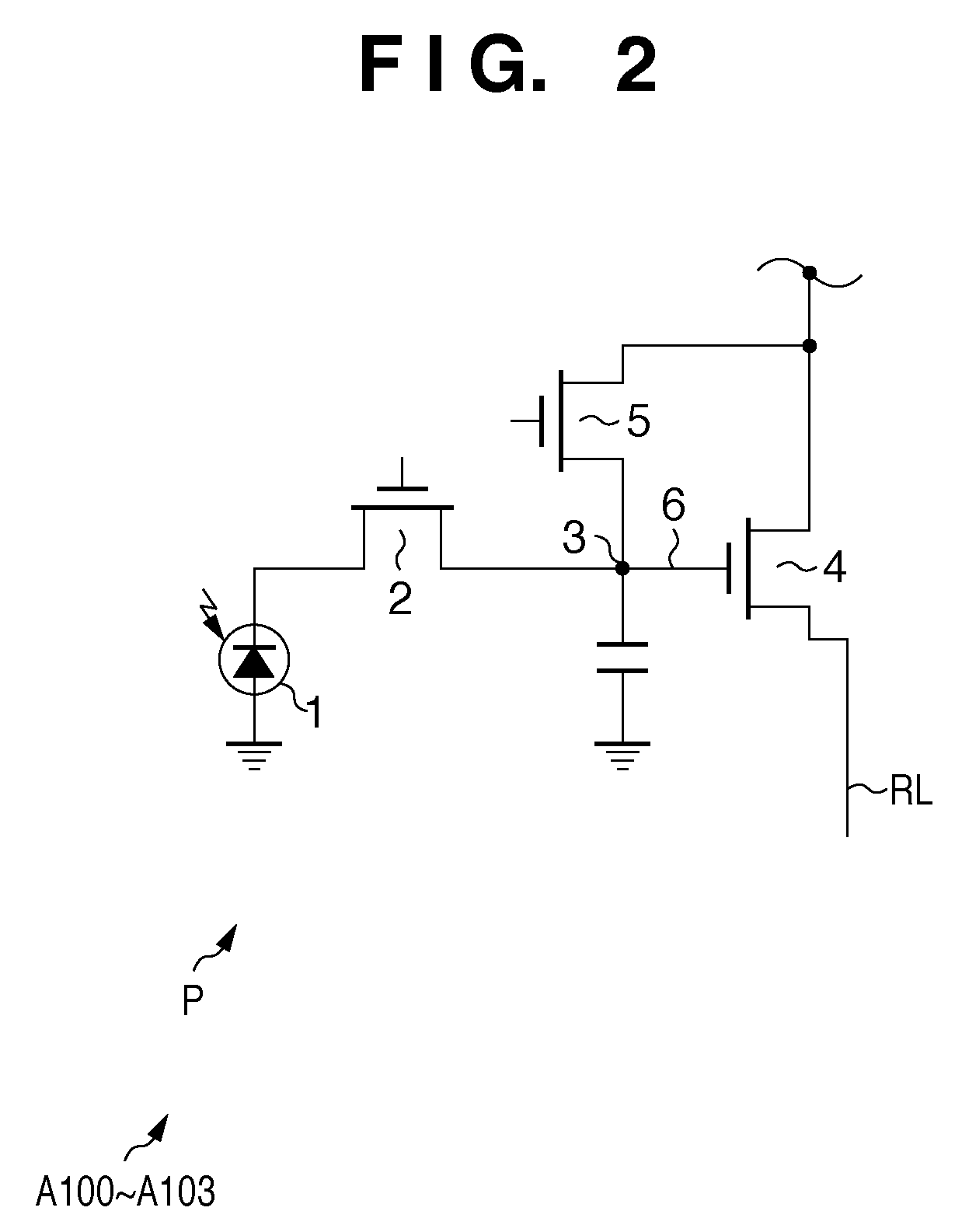
[0067]An image sensing apparatus 200 according to the second embodiment of the present invention will be explained. A difference from the first embodiment will be mainly explained.
[0068]As shown in FIG. 5, the image sensing apparatus 200 is different from the first embodiment in the layout of each pixel P in OB areas A101 to A103. In FIG. 5, C represents the layout of each pixel in the OB areas A101 to A103. In FIG. 5, D represents the layout of each pixel in an effective area A100.
[0069]In C and D of FIG. 5, portions surrounded by broken lines are gates 241a and 41b of amplification transistors 204a and 4b.
[0070]Assume that the gate widths of amplification transistors 4 in the OB areas A101 to A103 and effective area A100 are increased from W2 to W1 (while keeping the gate lengths unchanged). In this case, to keep the pixel area constant, the light-receiving areas of photoelectric converters 1 in the OB areas A101 to A103 and effective area A100 are decreased respectively. Although t
Example
[0076]An image sensing apparatus 300 according to the third embodiment of the present invention will be explained. A difference from the first embodiment will be mainly explained.
[0077]As shown in FIG. 6, the image sensing apparatus 300 is different from the first embodiment in the layout of each pixel P in OB areas A101 to A103. In FIG. 6, E and G represent the layout and sectional structure of each pixel in the OB areas A101 to A103. In FIG. 6, F and H represent the layout and sectional structure of each pixel in an effective area A100.
[0078]In FIG. 6, G represents a section of an amplification transistor 304a taken along the line O-O′ in the OB areas A101 to A103. In FIG. 6, H represents a section of an amplification transistor 4b taken along the line P-P′ in the effective area A100.
[0079]It is known that the gate insulating film capacitance (gate capacitance) Cox per unit area is inversely proportional to the thickness of the gate insulating film. That is, 1 / f noise is proportion
PUM
 Abstract
Description
Claims
Application Information
 - R&D Engineer
- R&D Manager
- IP Professional
- Industry Leading Data Capabilities
- Powerful AI technology
- Patent DNA Extraction
Browse by: Latest US Patents, China's latest patents, Technical Efficacy Thesaurus, Application Domain, Technology Topic.
© 2024 PatSnap. All rights reserved.Legal|Privacy policy|Modern Slavery Act Transparency Statement|Sitemap