Image sensor with epitaxially self-aligned photo sensors

Inactive Publication Date: 2011-07-14
OMNIVISION TECH INC
View PDF6 Cites 12 Cited by
  • Summary
  • Abstract
  • Description
  • Claims
  • Application Information

AI Technical Summary

Problems solved by technology

As CIS continue to miniaturize, the area of their pixels and principally their photodiode regions shrink, which results in less capacity to intercept light and hold photogenerated charge.
Additionally, as backside illuminated

Method used


Image

  • Image sensor with epitaxially self-aligned photo sensors
  • Image sensor with epitaxially self-aligned photo sensors
  • Image sensor with epitaxially self-aligned photo sensors

Examples


Embodiment Construction

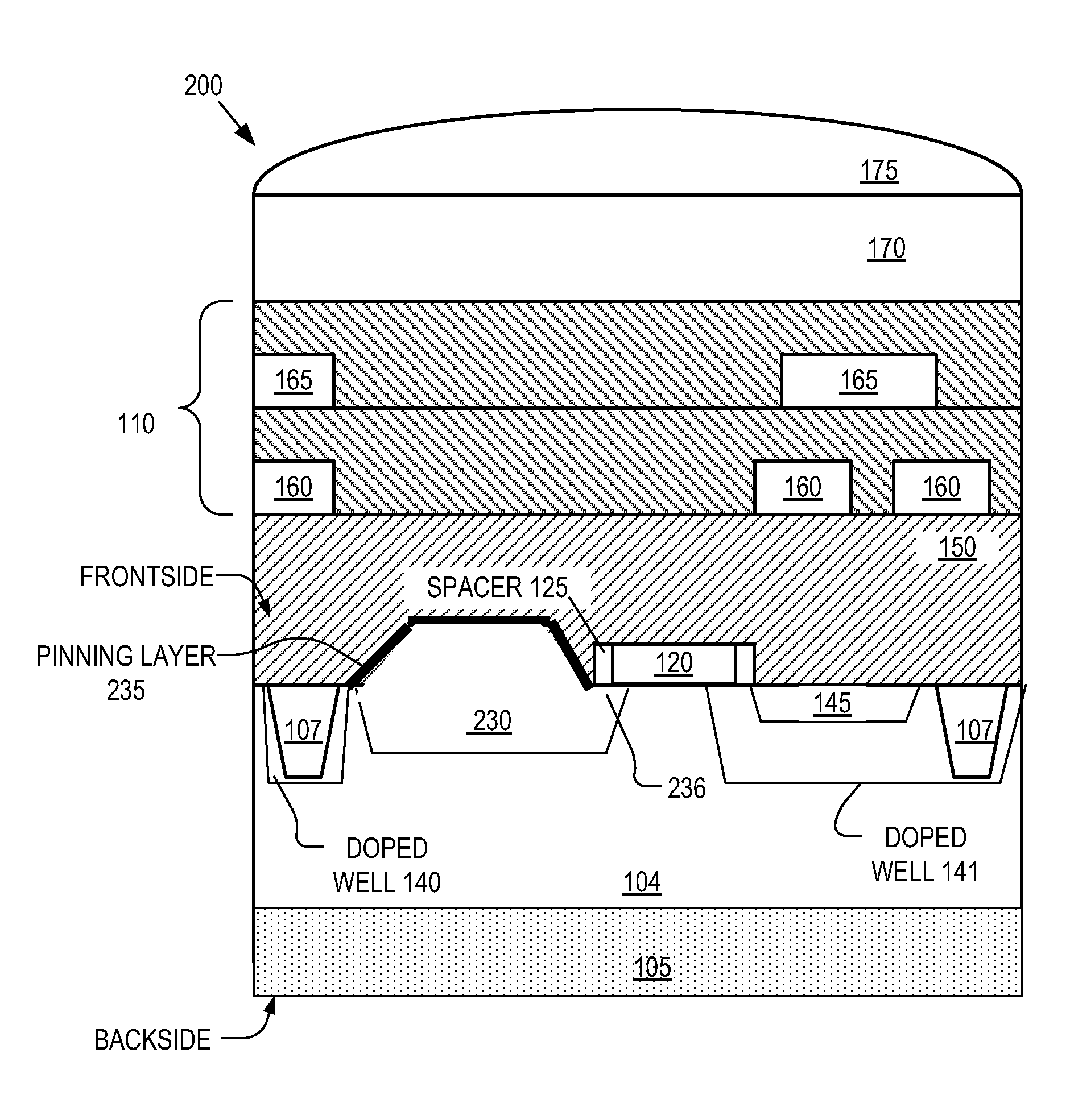
[0011]Embodiments of a pixel, an image sensor, an imaging system, and methods of fabrication of a pixel, image sensor, and imaging system having improved image lag, noise, and long wavelength sensitivity characteristics are described herein. In the following description numerous specific details are set forth to provide a thorough understanding of the embodiments. One skilled in the relevant art will recognize, however, that the techniques described herein can be practiced without one or more of the specific details, or with other methods, components, materials, etc. In other instances, well-known structures, materials, or operations are not shown or described in detail to avoid obscuring certain aspects. For example, although not illustrated, it should be appreciated that image sensor pixels may include a number of material layers disposed on the front side or backside (e.g., pixel circuitry, dielectric layers, metal stacks, color filters, microlenses, etc.), as well as other conventi


PUM


Abstract

An image sensor pixel includes a substrate doped to have a first conductivity type. A first epitaxial layer is disposed over the substrate and doped to also have the first conductivity type. A transfer transistor gate is formed on the first epitaxial layer. An epitaxially grown photo-sensor region is disposed in the first epitaxial layer and has a second conductivity type. The epitaxially grown photo-sensor region includes an extension region that extends under a portion of the transfer transistor gate.

Description


Claims


Application Information

Patent Timeline
Owner OMNIVISION TECH INC
Why Eureka
Try Eureka