Schottky diode
a diode and diode technology, applied in the field of electronic devices, can solve the problems of occupying space, requiring additional masking steps for fabrication of such a guard ring, and having poor reverse leakage characteristics
- Summary
- Abstract
- Description
- Claims
- Application Information
AI Technical Summary
Benefits of technology
Problems solved by technology
Method used
Image

Examples
second embodiment
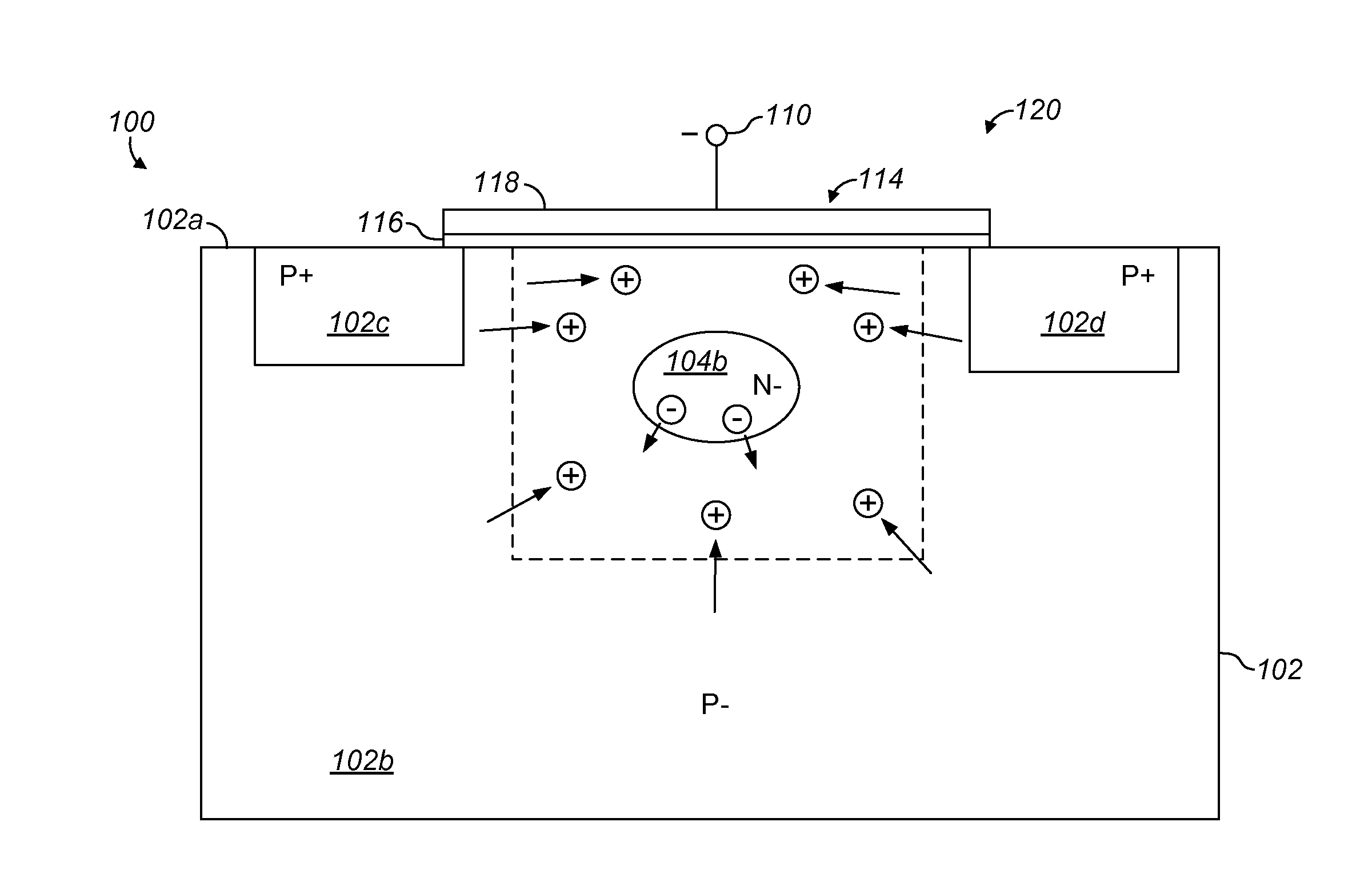
[0037]FIG. 3 shows a plan view of a Schottky diode 200. Elements of the Schottky diode 200 that are similar to or the same as those of the Schottky diode 100 are denoted by the same reference numerals, and description thereof is not repeated. FIG. 4A shows a cross-sectional view of the Schottky diode 200 taken along section lines 4A-4A, and FIG. 4B shows a cross-sectional view of the Schottky diode 200 taken along section lines 4B-4B.
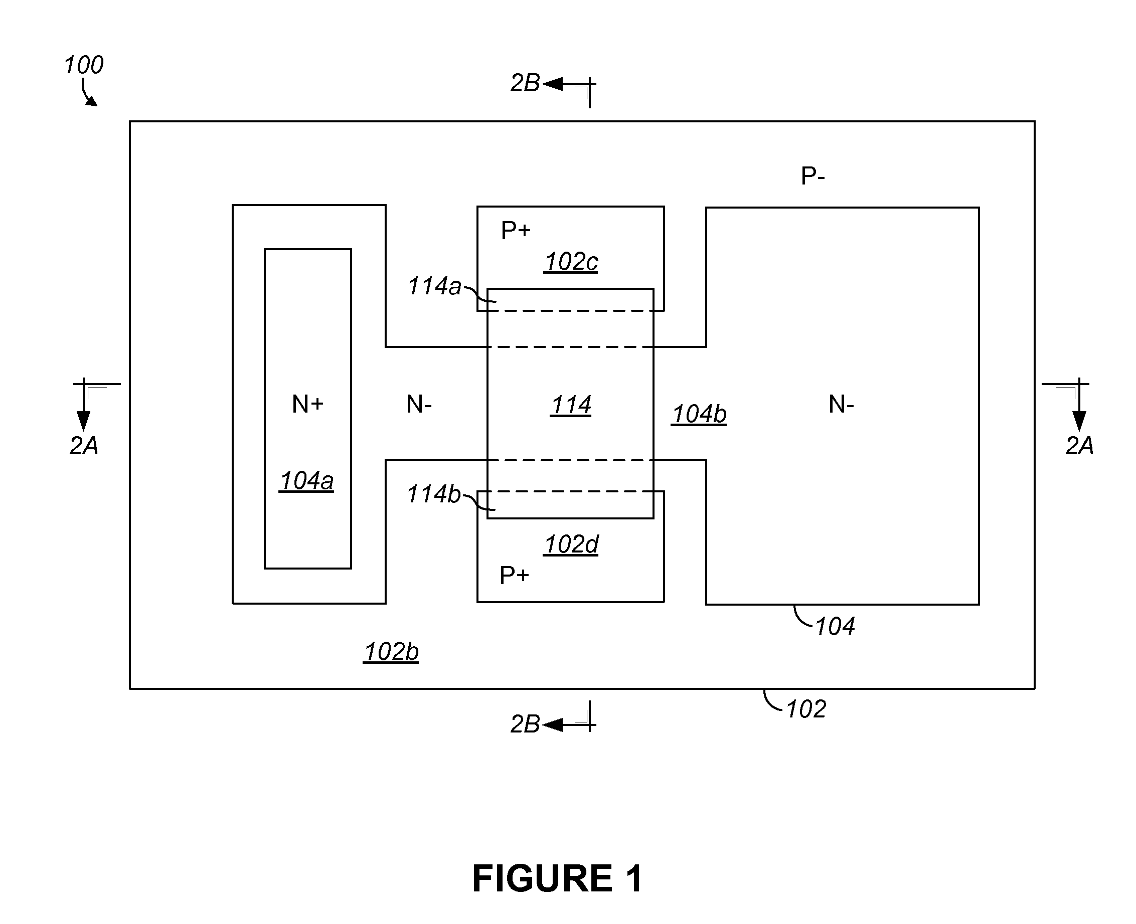
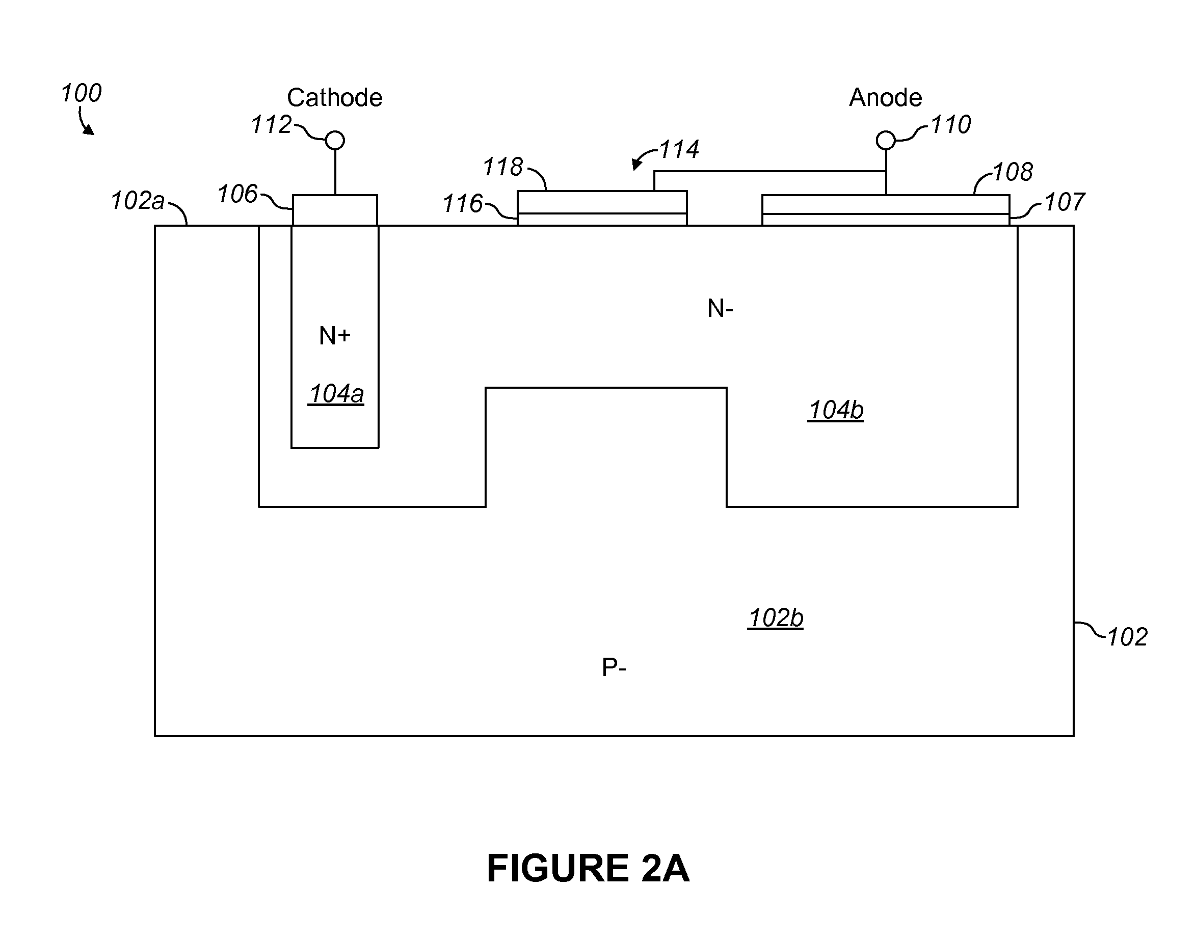
[0038]The Schottky diode 200 includes a substrate 202, which can also be referred to as well 202. The substrate 202 is composed of semiconductor material of a first conductivity type, typically P-type conductivity. The substrate 202 is formed within a well of a semiconductor substrate 204, typically silicon, of second conductivity type, typically N-type conductivity. The semiconductor substrate 204 has a contact face 102a. The drift channel 104 is also of the second conductivity type, typically N-type conductivity, and is formed in a first portion 202b of
third embodiment
[0041]FIG. 5 shows a plan view of a Schottky diode 300. Elements of the Schottky diode 300 that are similar to or the same as those of the Schottky diode 100 are denoted by the same reference numerals, and description thereof is not repeated.
[0042]The construction and operation of the Schottky diode 300 is the same as described above in connection with the Schottky diode 100, except that the Schottky diode 300 includes a plurality pinch-off mechanisms 120a-120c. Thus, while not shown in FIG. 5, the Schottky diode 300 can include an anode 110 and cathode 112 that are the same as those shown and described for Schottky diode 100, including an ohmic contact layer 106 disposed over the first portion 104a of the drift channel 104, and a Schottky barrier 107 and metal layer 108 disposed over the second portion 104b of the drift channel 104.
[0043]In the embodiment shown in FIG. 5, the second portion 104b of the drift channel 104 includes three branches 104b′, 104b″, and 104b′″ that extend betw
PUM
 Abstract
Description
Claims
Application Information
 - R&D Engineer
- R&D Manager
- IP Professional
- Industry Leading Data Capabilities
- Powerful AI technology
- Patent DNA Extraction
Browse by: Latest US Patents, China's latest patents, Technical Efficacy Thesaurus, Application Domain, Technology Topic.
© 2024 PatSnap. All rights reserved.Legal|Privacy policy|Modern Slavery Act Transparency Statement|Sitemap