Circuit and method for sensing a capacitance
a capacitance and capacitance technology, applied in the direction of converting the output of the sensor electrically/magnetically, amplifiers with semiconductor devices/discharge tubes, instruments, etc., can solve the problem of response speed
- Summary
- Abstract
- Description
- Claims
- Application Information
AI Technical Summary
Benefits of technology
Problems solved by technology
Method used
Image

Examples
first embodiment
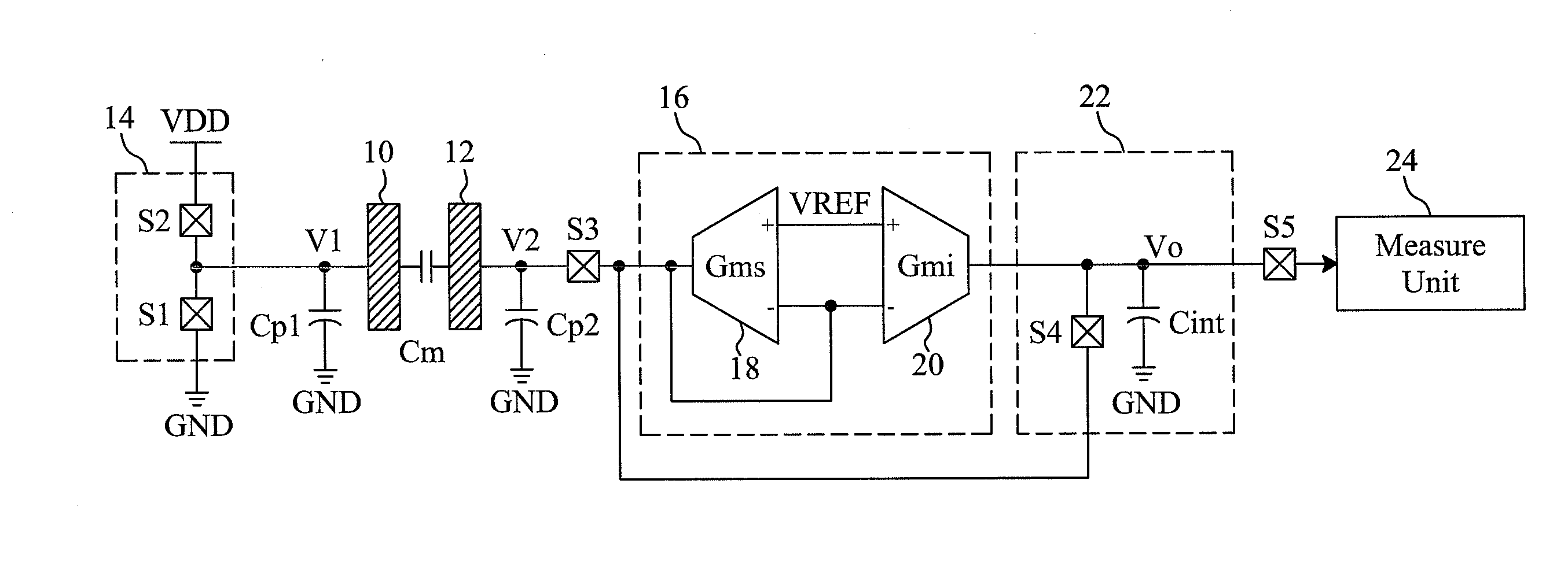
[0030]FIG. 1 is a circuit diagram of a first embodiment according to the present invention, in which a circuit for sensing the capacitance Cm between electrodes 10 and 12 includes a switching circuit 14, a transconductance amplifier mirror circuit 16, a charge calculation circuit 22 and a measure unit 24. In this embodiment, the switching circuit 14 includes switches S1 and S2 both connected to the electrode 10 to switch the voltage of the electrode 10 to a higher voltage level or a lower voltage level, for example, a supply voltage VDD and a ground voltage GND as shown in FIG. 1. A sensing switch S3 is connected between the other electrode 12 and the transconductance amplifier mirror circuit 16, controlled to connect the first output port of the transconductance amplifier mirror circuit 16 to the electrode 12. The transconductance amplifier mirror circuit 16 includes two common input transconductance amplifiers 18 and 20, one of the common input ports is applied with a reference volta
second embodiment
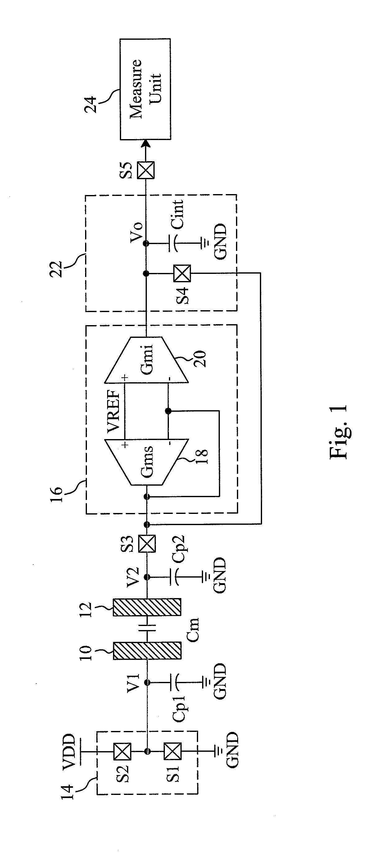
[0031]FIG. 2 is a circuit diagram of a second embodiment according to the present invention, whose operational modes and principles are similar to those of the embodiment depicted in FIG. 1. In this embodiment, the initialization switch S4 and the capacitor Cint in the charge calculation circuit 26 are shunt to each other between the output port of the transconductance amplifier 20 and the ground GND. Therefore, when the switch S4 is turned on prior to sensing the capacitance Cm, the voltage Vo of the capacitor Cint is initialized to the ground voltage GND.
[0032]FIG. 3 is a timing diagram for the circuits depicted in FIGS. 1 and 2. The switches S1 and S2 are controlled by two non-overlapping clocks. In the initial phase P0, the switches S2, S3 and S4 are turned on to set the voltage V1 of the electrode 10 to the supply voltage VDD, and the voltage V2 of the electrode 12 to the reference voltage VREF, and initialize the voltage Vo of the capacitor Cint either to the reference voltage VR
third embodiment
[0033]FIG. 4 is a circuit diagram of a third embodiment according to the present invention, which has the same circuit as that of FIG. 1 except that the capacitor Cint in the charge calculation circuit 28 is connected between the output port of the transconductance amplifier 20 and the voltage source VDD. Prior to sensing the capacitance Cm, the initialization switch S4 is turned on to initialize the voltage Vo of the capacitor Cint to the reference voltage VREF. At the beginning of sensing the capacitance Cm, the voltage V1 of the electrode 10 changes responsive to the switching of the switches S1 and S2 in the switching circuit 14. When the voltage V1 is pulled high, in order to sustain the voltage V2 at the reference voltage VREF, the transconductance amplifier 18 will drain charges from the electrode 12 responsive to the difference between the voltage V2 and the reference voltage VREF, and the transconductance amplifier 20 will also drain a proportional amount of charges from the c
PUM
 Abstract
Description
Claims
Application Information
 - R&D Engineer
- R&D Manager
- IP Professional
- Industry Leading Data Capabilities
- Powerful AI technology
- Patent DNA Extraction
Browse by: Latest US Patents, China's latest patents, Technical Efficacy Thesaurus, Application Domain, Technology Topic.
© 2024 PatSnap. All rights reserved.Legal|Privacy policy|Modern Slavery Act Transparency Statement|Sitemap