System and method for reducing metastability in CMOS flip-flops
- Summary
- Abstract
- Description
- Claims
- Application Information
AI Technical Summary
Benefits of technology
Problems solved by technology
Method used
Image


Examples
first embodiment
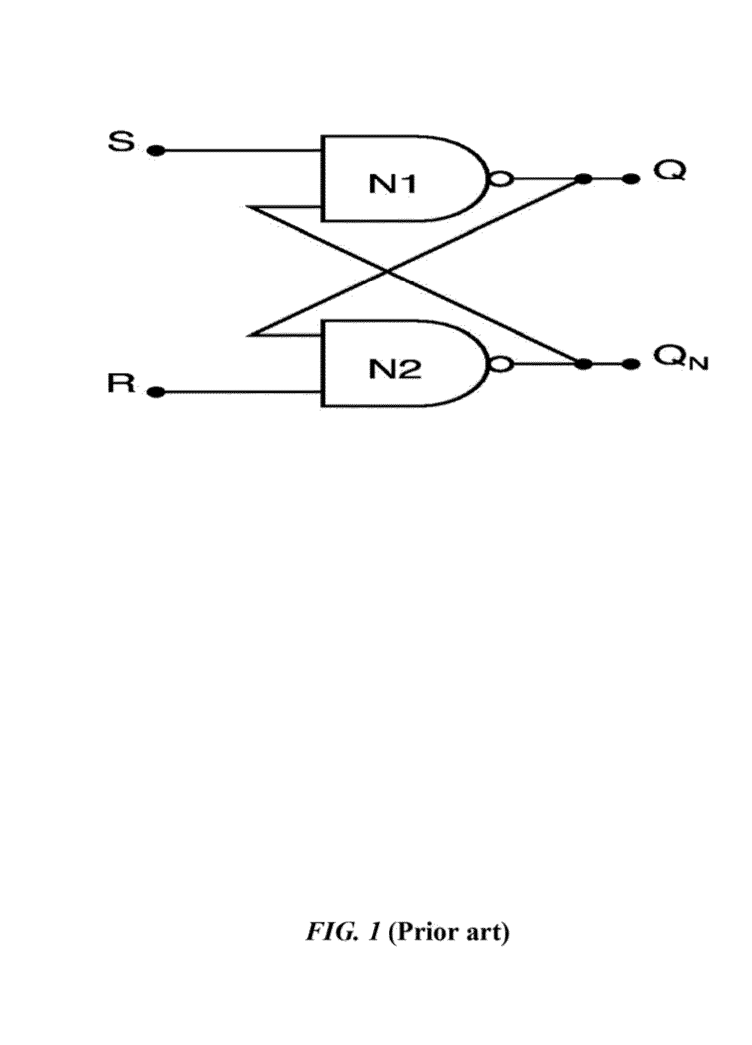
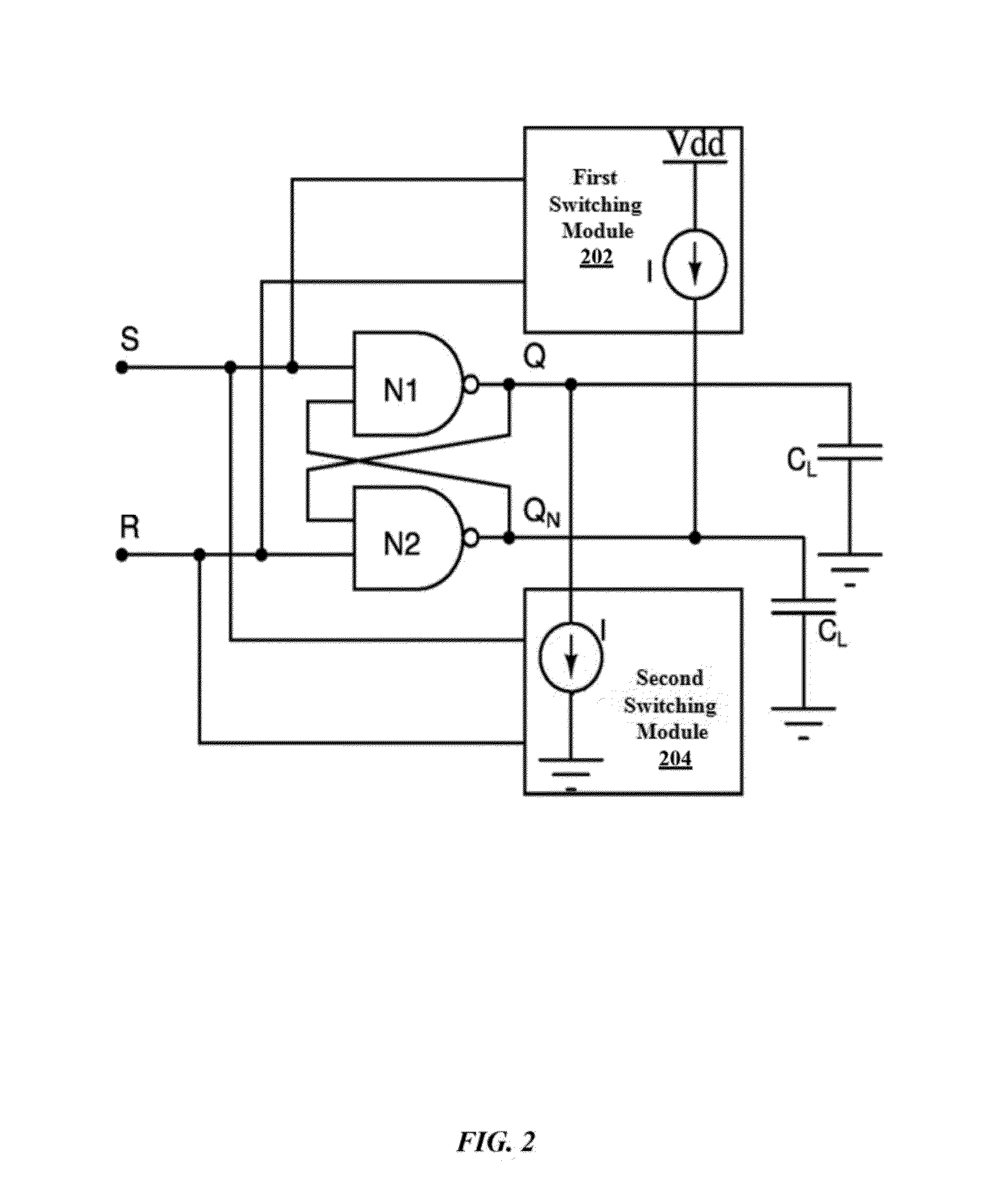
[0019]The first embodiment herein provides a circuit for reducing the metastability of the CMOS SR flip flop. The circuit comprises a first switching module and a second switching module that are operatively coupled to a first and second output terminal of the CMOS SR flip-flop. The output terminals are configured to receive injected current from the switching modules at mutually opposite directions respectively during permissible mid-range voltages of the output terminals. The switching modules are configured to drive the output terminals into a predetermined state of zero and a predetermined stable state of Vdd by utilizing the injected current onto the output terminals of the CMOS SR flip-flop. The switching modules further configured to divert a metastable point of the CMOS SR flip-flop from a corresponding metastable voltage into known stable states along with corresponding voltage noise, current noise, and cross-talk noise. Thus, the metastability of the CMOS SR flip-flop is redu
second embodiment
[0020]The second embodiment herein provides a method for reducing the metastability of the e CMOS SR flip-flop. The method includes injecting current onto the first and second output terminals of the CMOS SR flip-flop at mutually opposite directions during permissible mid-range voltages of the output terminals. Further, the method includes driving the output terminals of the CMOS SR flip-flop into the predetermined state of zero and predetermined stable state of Vdd by utilizing the currents injected onto the output terminals. Furthermore, the method includes diverting the metastable point of the CMOS SR flip-flop from the corresponding metastable voltage and thereby reducing the metastability of the CMOS SR flip-flop.
third embodiment
[0021]The third embodiment herein provides a circuit for reducing the metastability of the positive edge triggered D flip-flop.
[0022]These and other aspects of the embodiments herein will be better appreciated and understood when considered in conjunction with the following description and the accompanying drawings. It should be understood, however, that the following descriptions, while indicating the preferred embodiments and numerous specific details thereof, are given by way of an illustration and not of a limitation. Many changes and modifications may be made within the scope of the embodiments herein without departing from the spirit thereof, and the embodiments herein include all such modifications.
PUM
 Abstract
Description
Claims
Application Information
 - R&D Engineer
- R&D Manager
- IP Professional
- Industry Leading Data Capabilities
- Powerful AI technology
- Patent DNA Extraction
Browse by: Latest US Patents, China's latest patents, Technical Efficacy Thesaurus, Application Domain, Technology Topic.
© 2024 PatSnap. All rights reserved.Legal|Privacy policy|Modern Slavery Act Transparency Statement|Sitemap