Method for manufacturing solid-state image sensor

Active Publication Date: 2016-09-15
CANON KK
View PDF4 Cites 2 Cited by
  • Summary
  • Abstract
  • Description
  • Claims
  • Application Information

AI Technical Summary

Benefits of technology

[0007]The present invention provides a technique advanta

Problems solved by technology

When forming each light-guide portion, a temperature change may cause a stress between the respectiv

Method used


Image

  • Method for manufacturing solid-state image sensor
  • Method for manufacturing solid-state image sensor
  • Method for manufacturing solid-state image sensor

Examples


Embodiment Construction

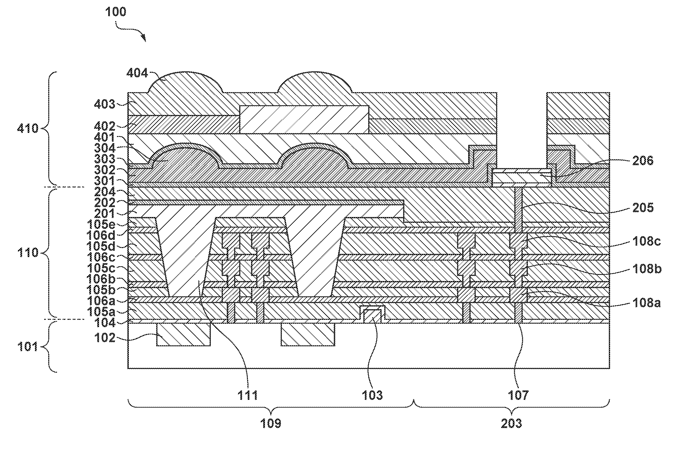
[0014]FIG. 1 is a schematic view showing an example of the structure of a solid-state image sensor (to be referred to as a “solid-state image sensor 100”) according to the present invention. The solid-state image sensor 100 includes, for example, a semiconductor substrate 101 made of silicon or the like, a structure 110 which includes an insulating member and a metal member (an interconnection, a plug, or the like) formed in the insulating member, and a structure 410 which includes an optical element for condensing incident light. The solid-state image sensor 100 also includes an imaging region 109 in which a plurality of pixels are arrayed and a peripheral region 203 which surrounds the imaging region 109 and in which a circuit configured to process a pixel signal is arranged.

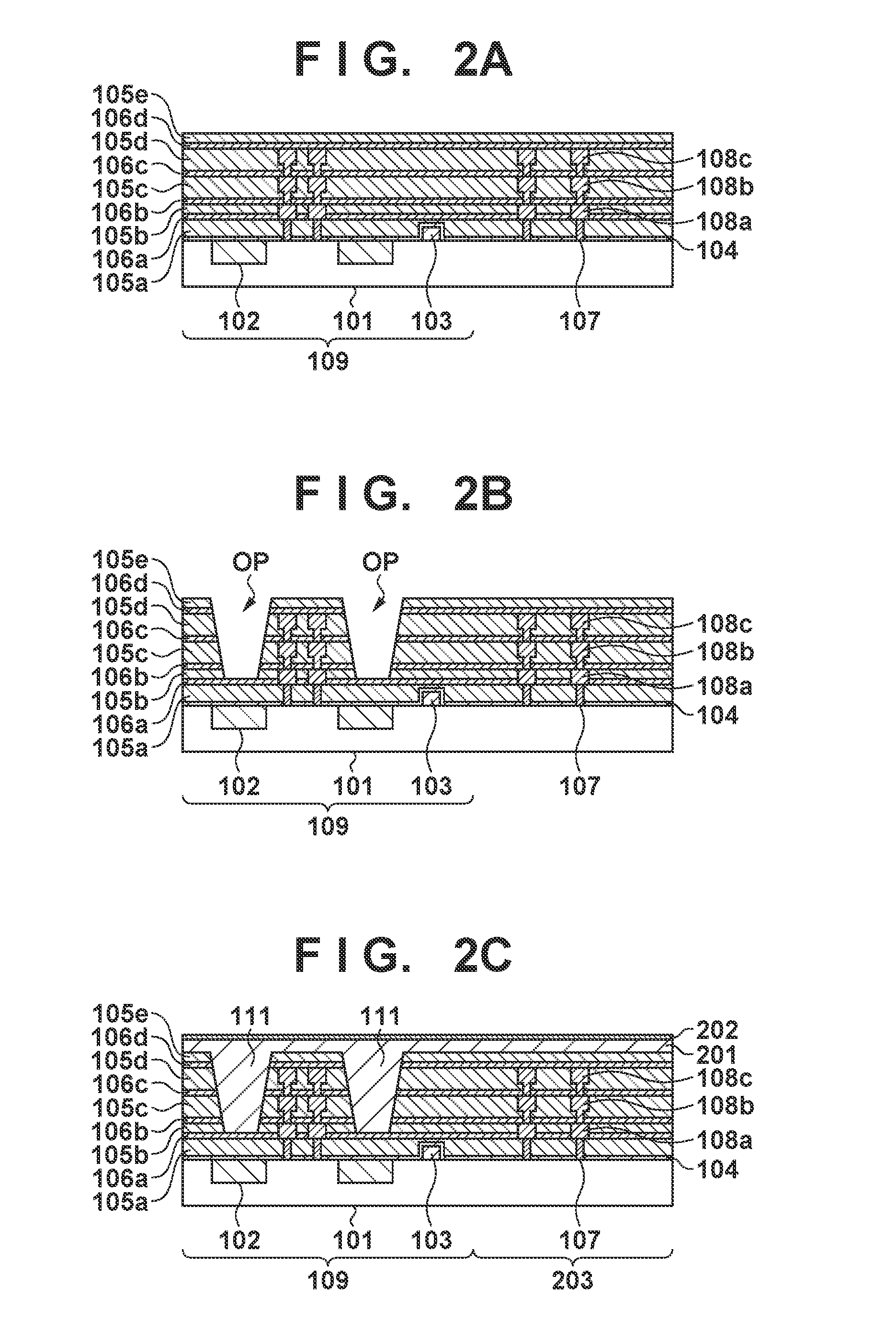
[0015]In the imaging region 109, photoelectric conversion portions 102 are formed in the substrate 101. A transistor configured to read out or process the pixel signal is also formed in the substrate 101. A gate


PUM


Abstract

A method for manufacturing a solid-state image sensor, the method comprising preparing a substrate including a photoelectric conversion portion, forming, on the substrate, a structure which includes a first member made of a material containing silicon oxide and a second member arranged on the first member and made of a material containing silicon carbide, forming an opening in a position above the photoelectric conversion portion in the structure by removing a part of the first and the second members, and forming a transparent member in the opening, wherein the second member is formed at a first temperature and the transparent member is formed at a second temperature lower than the first temperature.

Description


Claims


Application Information

Patent Timeline
Owner CANON KK
Why Eureka
Try Eureka