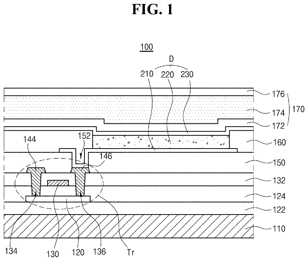
Organic light emitting diode and organic light emitting device having the diode
a light-emitting diode and organic technology, applied in the direction of solid-state devices, chemistry apparatuses and processes, and light-emitting compositions, can solve the problems of unsatisfactory lifetime and low color purity of the blue phosphorescent material used in the light-emitting device, and achieve the effect of improving color purity and luminous efficiency
- Summary
- Abstract
- Description
- Claims
- Application Information
AI Technical Summary
Benefits of technology
Problems solved by technology
Method used
Image

Examples
experimental example 1
evel of Compound
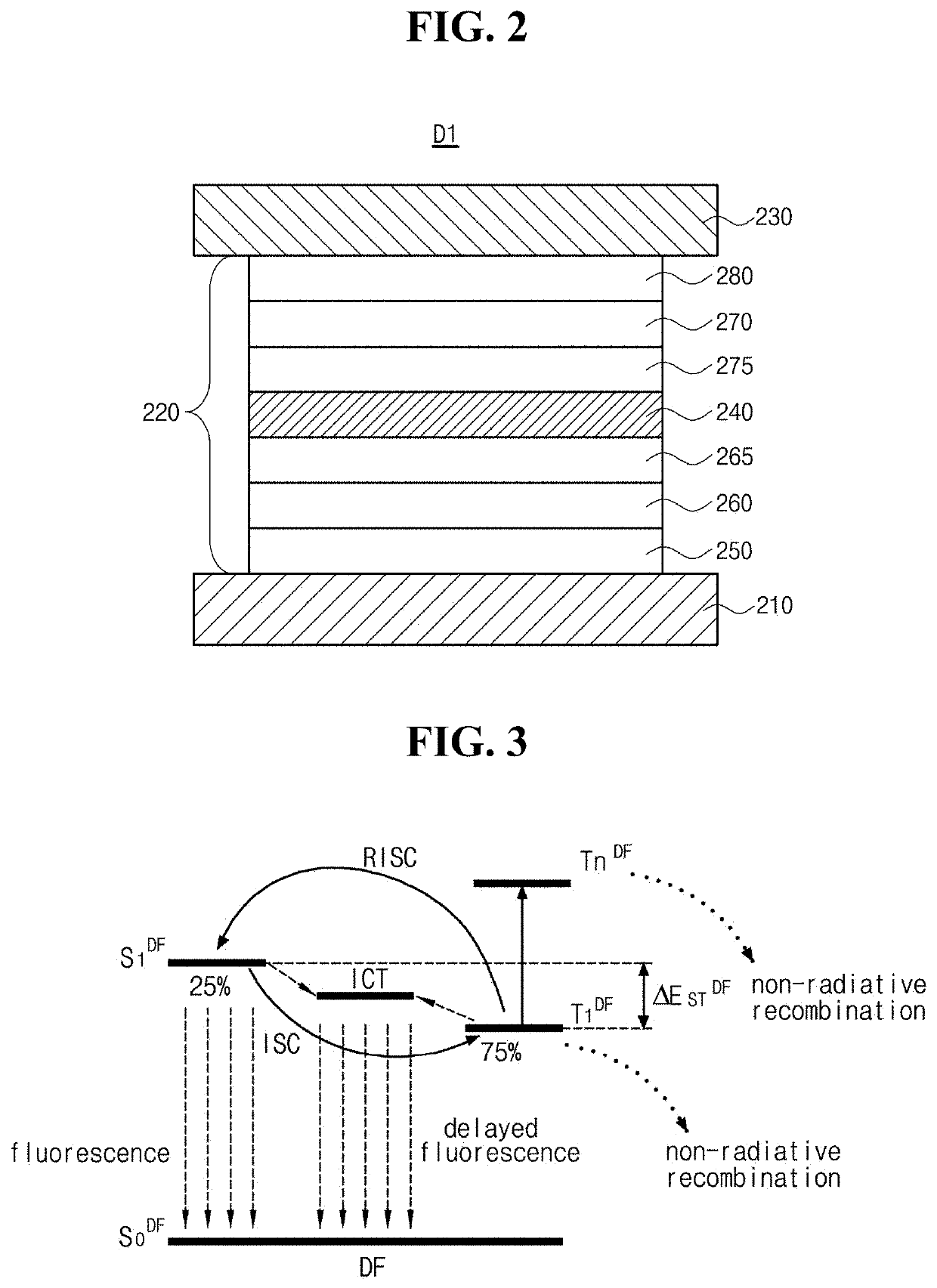
[0222]Energy levels such as HOMO energy levels, LUMO energy levels, excited singlet energy levels S1 and excited triplet energy levels T1 for mCBP as a host, the compounds 1-3 in Chemical Formula 4 as a first delayed fluorescent material, the compound M-1 in Chemical Formula 5, B3PyMPM as the HBL material and the reference compound (Ref) below, which is triazine-based delayed fluorescent material, were evaluated. Table 1 below indicates the evaluation results.
[0223][Reference Compound]
TABLE 1Energy Level of CompoundHOMOLUMOS1T1Compound(eV)(eV)(eV)(eV)Host (mCBP)−5.9−2.43.22.9DF1Compound 1−5.9−3.3—2.4Compound 2−5.9−3.2—2.4Compound 3−5.9−3.2—2.3Reference compound−5.6−3.0—2.6DF2Compound M-1−5.9−3.0—2.6HBLB3PYMPM—−2.7HOMO: Film (100 nm / ITO), by AC3;LUMO: calculated from film absorption edge;T1: Calculated by Gaussian ED-DFT(time-dependent density functional theory)
example 1 (
Ex. 1): Fabrication of OLED
[0224]An OLED comprising an EML into which mCBP as a host, Compound 1 as a first delayed fluorescent material and Compound M-1 as a second delayed fluorescent material was introduced was fabricated. ITO substrate was washed by UV-Ozone treatment before using, and was transferred to a vacuum chamber for depositing emission layer. Subsequently, an anode, an emission layer and a cathode were deposited by evaporation from a heating boat under 10−6 Torr vacuum condition as the following order:
[0225]An anode (ITO, 50 nm); a HIL (HAT-CN, 7 nm); a HTL (NPB, 18 nm); an EBL (TAPC, 15 nm), an EML (mCBP: Compound 1: Compound M-1=60:20:20 by weight ratio, 35 nm); a HBL (B3PYMPM, 10 nm); an ETL (TPBi, 25 nm), an EIL (LiF, 5 nm); and a cathode (Al, 100 nm).
[0226]And then, cappling layer (CPL) was deposited over the cathode and the device was encapsulated by glass. After deposition of emissive layer and the cathode, the OLED was transferred from the deposition chamber to a d
examples 2-4 (
Ex. 2˜4): Fabrication of OLED
[0227]An OLED was fabricated using the same materials as Example 1, except adjusting the weight ratio of mCBP: Compound 1: Compound M-1 to 80:10:10 (Ex. 2), 40:30:30 (Ex. 3) and 20:40:40 (Ex. 4), respectively.
PUM
 Abstract
Description
Claims
Application Information
 - R&D Engineer
- R&D Manager
- IP Professional
- Industry Leading Data Capabilities
- Powerful AI technology
- Patent DNA Extraction
Browse by: Latest US Patents, China's latest patents, Technical Efficacy Thesaurus, Application Domain, Technology Topic.
© 2024 PatSnap. All rights reserved.Legal|Privacy policy|Modern Slavery Act Transparency Statement|Sitemap