Array substrate, manufacturing method thereof, and display panel

Active Publication Date: 2021-11-25
SHENZHEN CHINA STAR OPTOELECTRONICS SEMICON DISPLAY TECH CO LTD
View PDF10 Cites 0 Cited by
  • Summary
  • Abstract
  • Description
  • Claims
  • Application Information

AI Technical Summary

Benefits of technology

[0054]The beneficial effects of the invention are: The present invention provides an array substrate, a manufacturing method of the array substrate, and a display panel. The array substrate comprises a substrate, a buffer layer, an active layer, a gate insulating layer, a gate layer, an interlayer dielectric layer, a source drain layer, and a planarization layer, The buffer layer is formed on a side of the substrate. The active layer is formed on a side of the buffer layer away from the substrate. The gate insulating layer is formed on the active layer and the buffer layer. The gate layer is formed on a side of the gate insulating layer away from the active layer and is patterned to form a gate. The interlayer dielectric layer is formed on the gate layer and the gate insulating layer. The source drain layer is form

Problems solved by technology

When the planarization layer is formed later, the step of filling the planarization layer is large, and the filling is not good, which affects the

Method used


Image

  • Array substrate, manufacturing method thereof, and display panel
  • Array substrate, manufacturing method thereof, and display panel
  • Array substrate, manufacturing method thereof, and display panel

Examples


Embodiment Construction

[0069]The following description of the various embodiments is provided with reference to the accompanying drawings. Directional terms, such as upper, lower, front, back, left, right, inner, outer, and lateral side, mentioned in the present invention are only for reference. Therefore, the directional terms are used for describing and understanding rather than limiting the present invention. In the figures, units having similar structures are used for the same reference numbers.

[0070]The present invention provides a manufacturing method of an array substrate to alleviate a technical problem that a planarization layer in a current array substrate is not well filled.

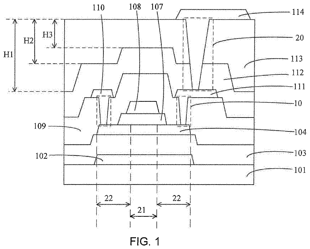
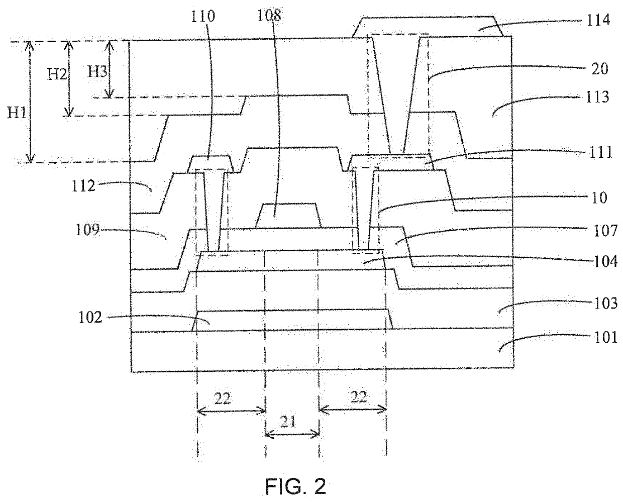
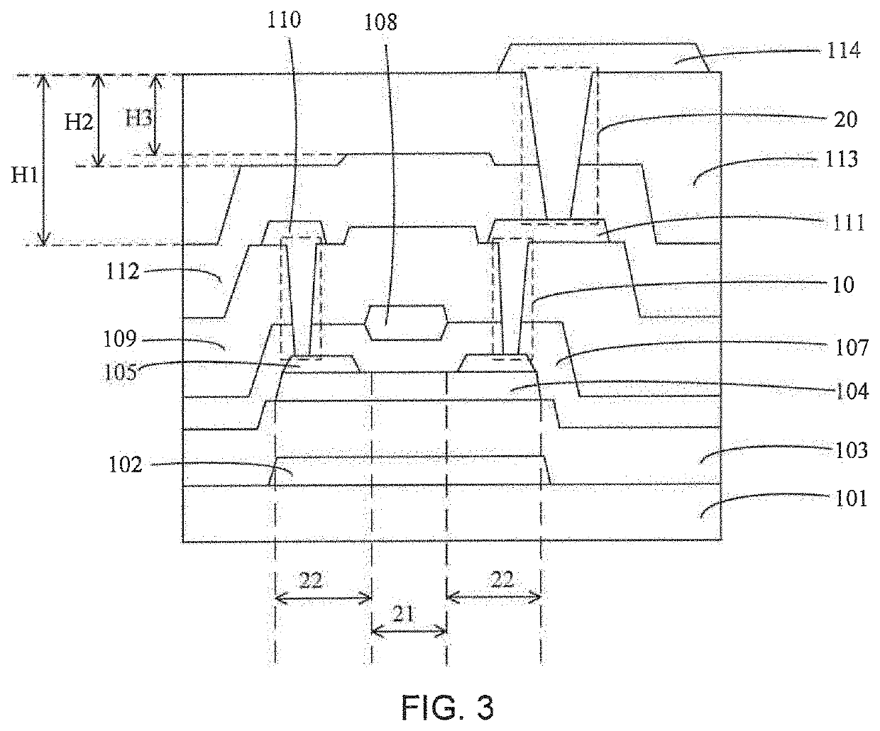
[0071]As shown in FIG. 2, the present invention provides an array substrate comprising a substrate 101, a buffer layer 103, an active layer 104, a gate insulating layer 107, a gate layer, an interlayer dielectric layer 109, a source drain layer, and a planarization layer 113.

[0072]The substrate 101 may be a rigid substrate or a


PUM


Abstract

The present invention provides an array substrate, a manufacturing method thereof, and a display panel. The array substrate includes a substrate, a buffer layer, an active layer, a gate insulating layer, a gate layer, an interlayer dielectric layer, a source drain layer, and a planarization layer. The gate insulating layer is formed on the active layer and the buffer layer. The interlayer dielectric layer is formed on the gate layer and the gate insulating layer. The source drain layer is patterned to form a source and a drain, and is connected to the active layer through via holes. The planarization layer in the present invention is easier to fill in.

Description


Claims


Application Information

Patent Timeline
Owner SHENZHEN CHINA STAR OPTOELECTRONICS SEMICON DISPLAY TECH CO LTD
Why Eureka
Try Eureka