Read circuit of nonvolatile semiconductor memory
a nonvolatile semiconductor and read circuit technology, applied in static storage, digital storage, instruments, etc., can solve the problems of inability to reduce the value icell in the first term on the right side, the inability to simultaneously achieve faster read operation and lower power consumption, and the inability to perform a fast read. , to achieve the effect of reducing the consumption of current and performing a fast read
- Summary
- Abstract
- Description
- Claims
- Application Information
AI Technical Summary
Benefits of technology
Problems solved by technology
Method used
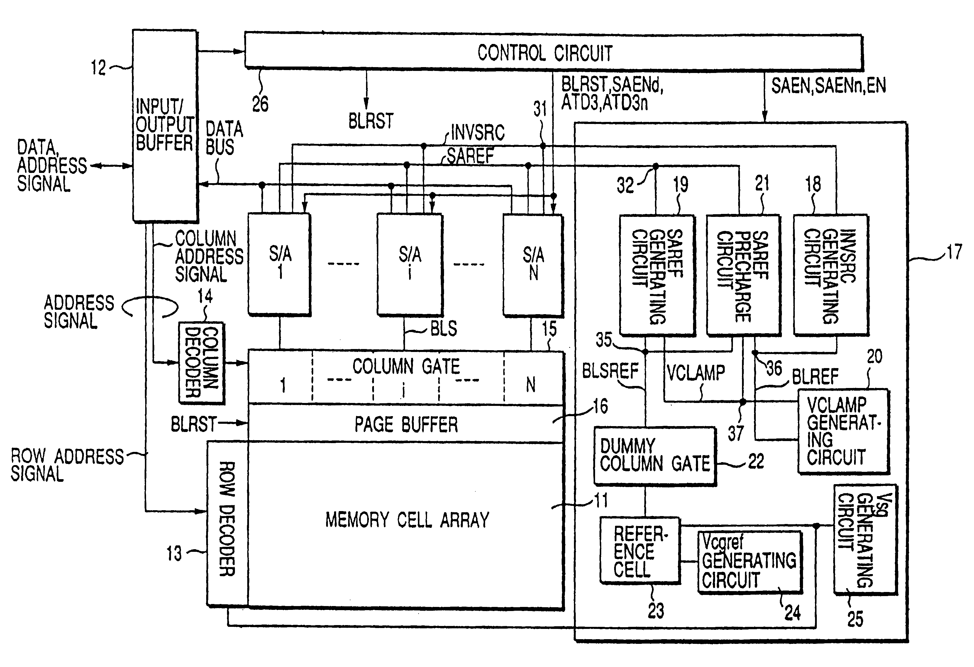
Image

Examples
modification 1
3.1. Modification 1
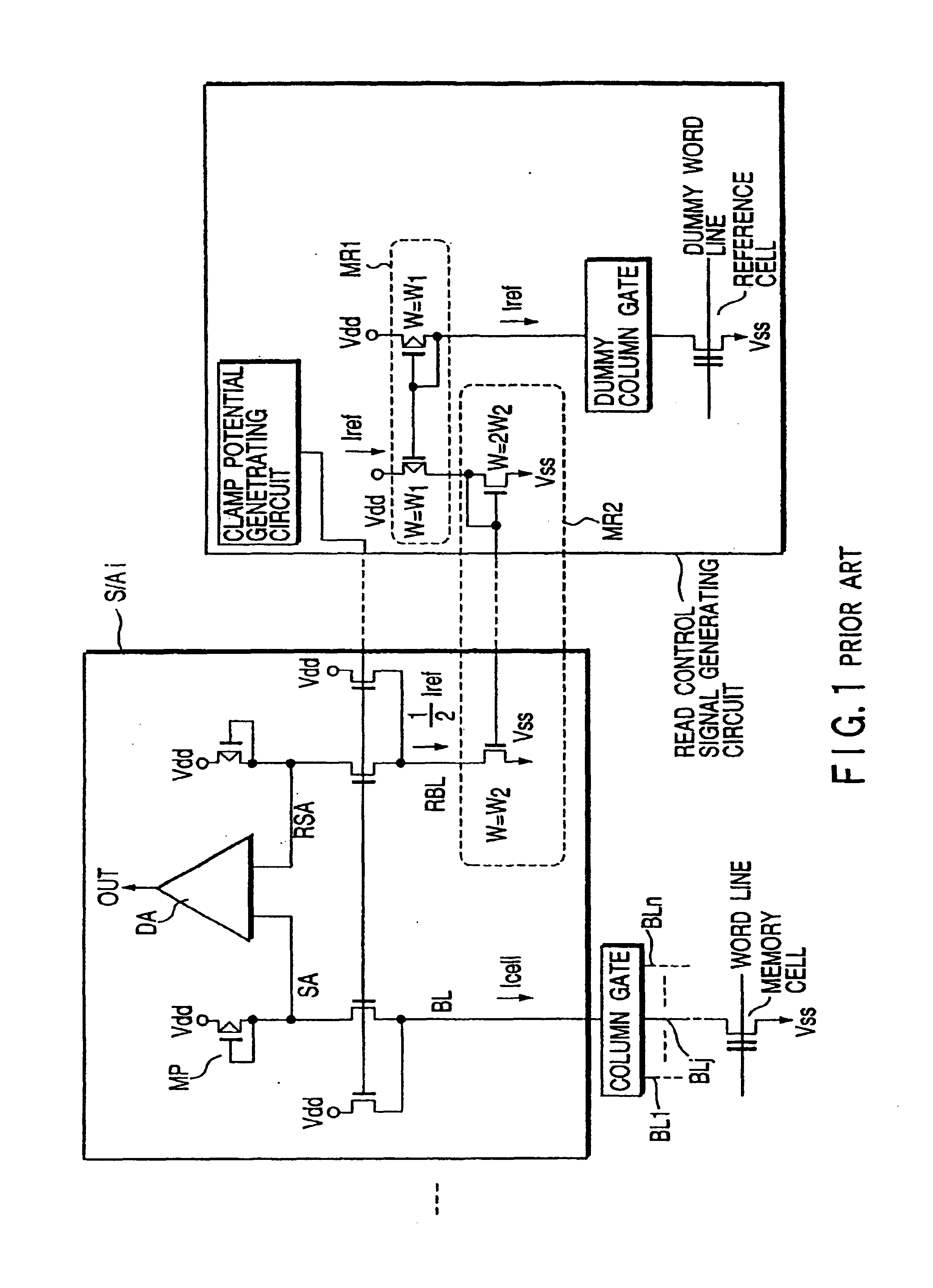
FIGS. 16 and 17 show main components of a read circuit according to the present invention.
This read circuit is characterized by the configuration of a precharge circuit for use in precharging and sensing the bit line BLj, as compared with the read circuit shown in FIGS. 6 and 7.
Specifically, in this modification, the sense amplifier S / Ai excludes the inverter INV2 as shown in FIG. 6. More specifically, the VCLAMP node 37 is connected directly to gates of MOS transistors MI1, MI2′.
In this configuration, as ATD3 transitions to “H” (in the bit line precharge period), the bit line BLj (BLS node 34 and SA node 33) is supplied with charges from the MOS transistor MI2′ to precharge the bit line BLj. The precharge level is determined by Vdd, the diode-connected MOS transistor ML4, and the like.
In the read circuit of this modification, since a constant potential is maintained at a gate of the MOS transistor MI2′ at all times, the MOS transistor MI2′ must be large in size (c
modification 2
3.2. Modification 2
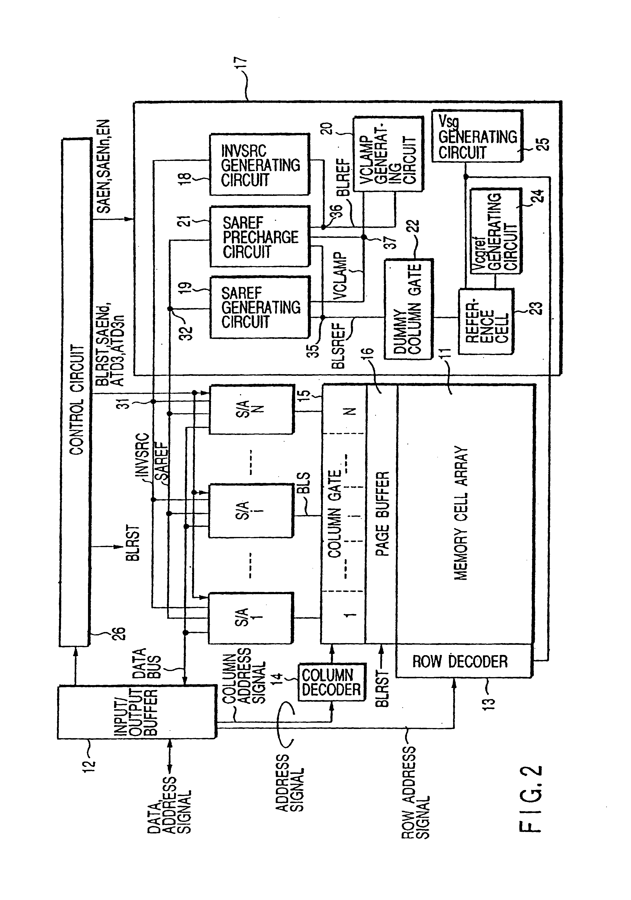
FIG. 18 shows main components of a read circuit according to the present invention.
In comparison with the read circuit of FIGS. 6 and 7, this read circuit is characterized in that the potential at the gate of the MOS transistor MI3 in the SAREF generating circuit 19 is generated by a mechanism similar to the inverter INV2 in FIG. 6.
Specifically, an inverter INV4 corresponds to the inverter INV2 in FIG. 6, and a charging circuit (comprised of MOS transistors MP13, MI6, ML5, MN15) corresponds to the precharge circuit (comprised of MOS transistors MP8, MI2, ML4, MN6) in FIG. 6.
The sense amplifier S / Ai of the read circuit shown in FIG. 18 is identical in internal configuration to the sense amplifier S / Ai shown in FIG. 6.
With the configuration described above, since a circuit for generating the potential at the gate of the MOS transistor MI1 (see FIG. 6) has completely the same configuration as a circuit for generating the potential at the gate of the MOS transistor M
PUM
 Abstract
Description
Claims
Application Information
 - R&D Engineer
- R&D Manager
- IP Professional
- Industry Leading Data Capabilities
- Powerful AI technology
- Patent DNA Extraction
Browse by: Latest US Patents, China's latest patents, Technical Efficacy Thesaurus, Application Domain, Technology Topic.
© 2024 PatSnap. All rights reserved.Legal|Privacy policy|Modern Slavery Act Transparency Statement|Sitemap