Method of manufacturing electro-optical device, electro-optical device, transferred chip, transfer origin substrate

a manufacturing method and technology of electrooptical devices, applied in the field of display devices, can solve the problems that the manufacturing cost may depend on the area, and achieve the effects of reducing the cost and production yield, reducing the cost of electronic devices, and constructing with low cos

Inactive Publication Date: 2007-01-30
SEIKO EPSON CORP
View PDF23 Cites 79 Cited by
  • Summary
  • Abstract
  • Description
  • Claims
  • Application Information

AI Technical Summary

Benefits of technology

This patent describes a new way to make optics that are less expensive than traditional methods. It also allows for the creation of displays that use these materials more efficiently.

Problems solved by technology

The technical problem addressed in this patent is how to reduce the costs associated with manufacturing displays used in electronic devices while maintaining their performance. This is achieved by separating the necessary components needed for each component of the display device, which requires a simpler and more efficient way than current methods.

Method used


Image

  • Method of manufacturing electro-optical device, electro-optical device, transferred chip, transfer origin substrate
  • Method of manufacturing electro-optical device, electro-optical device, transferred chip, transfer origin substrate
  • Method of manufacturing electro-optical device, electro-optical device, transferred chip, transfer origin substrate

Examples


Embodiment Construction

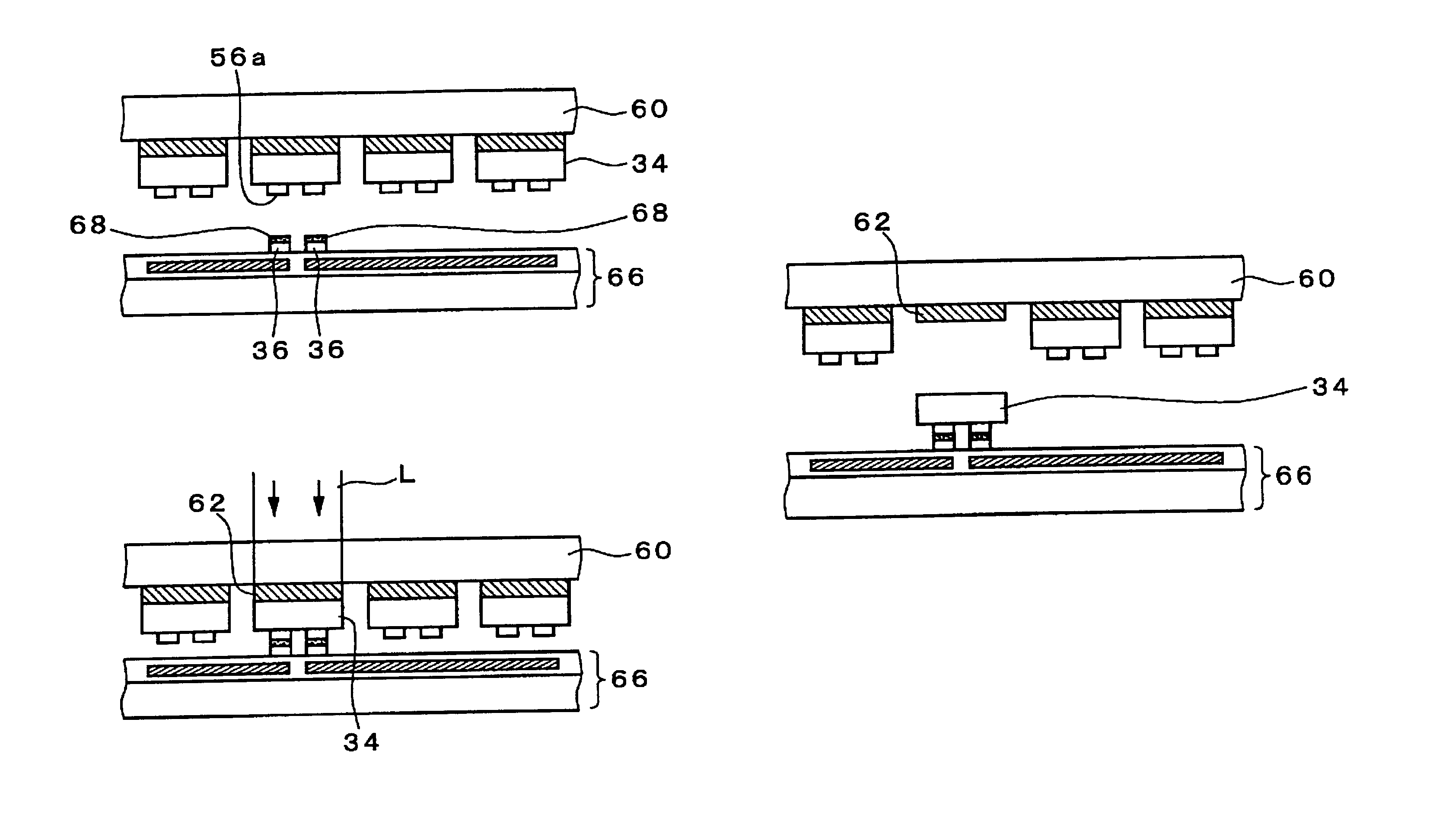
[0043]A structure and a manufacturing method of a display device to be driven with thin film transistors according to an exemplary embodiment of the present invention is described in detail below. In this exemplary embodiment, an organic EL display device is described as an example of the display device to be driven with thin film transistors.

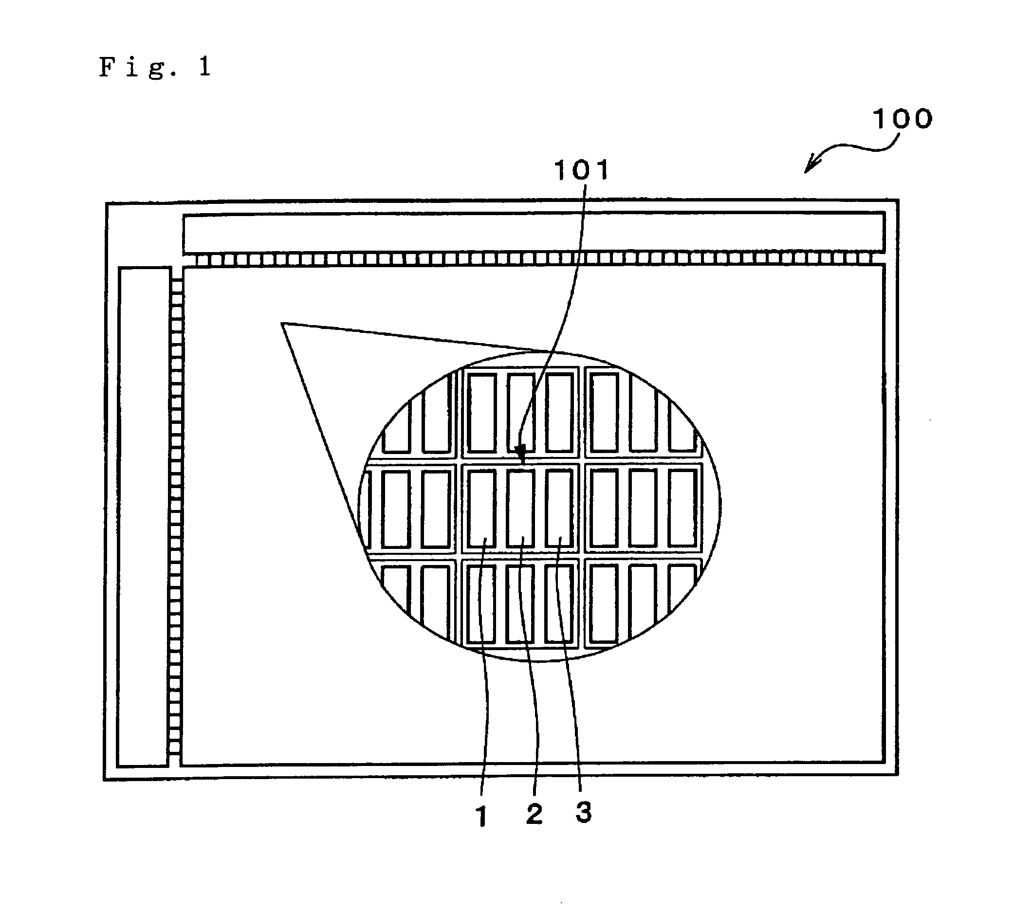
[0044]FIG. 1 is a schematic illustrating a configuration of the organic EL display device according to this exemplary embodiment. In the organic EL display device 100 shown in FIG. 1, a plurality of pixels (basic pixels) 101, each of which includes three-color pixels 1, 2, 3, is arranged in a matrix shape.

[0045]Among the color pixels, for example, the color pixel 1 corresponds to a red color, the color pixel 2 corresponds to a green color, and the color pixel 3 corresponds to a blue color. The respective pixels 101 are driven by chips having a drive circuit built in, the drive circuit including a plurality of thin film transistors (TFTs).
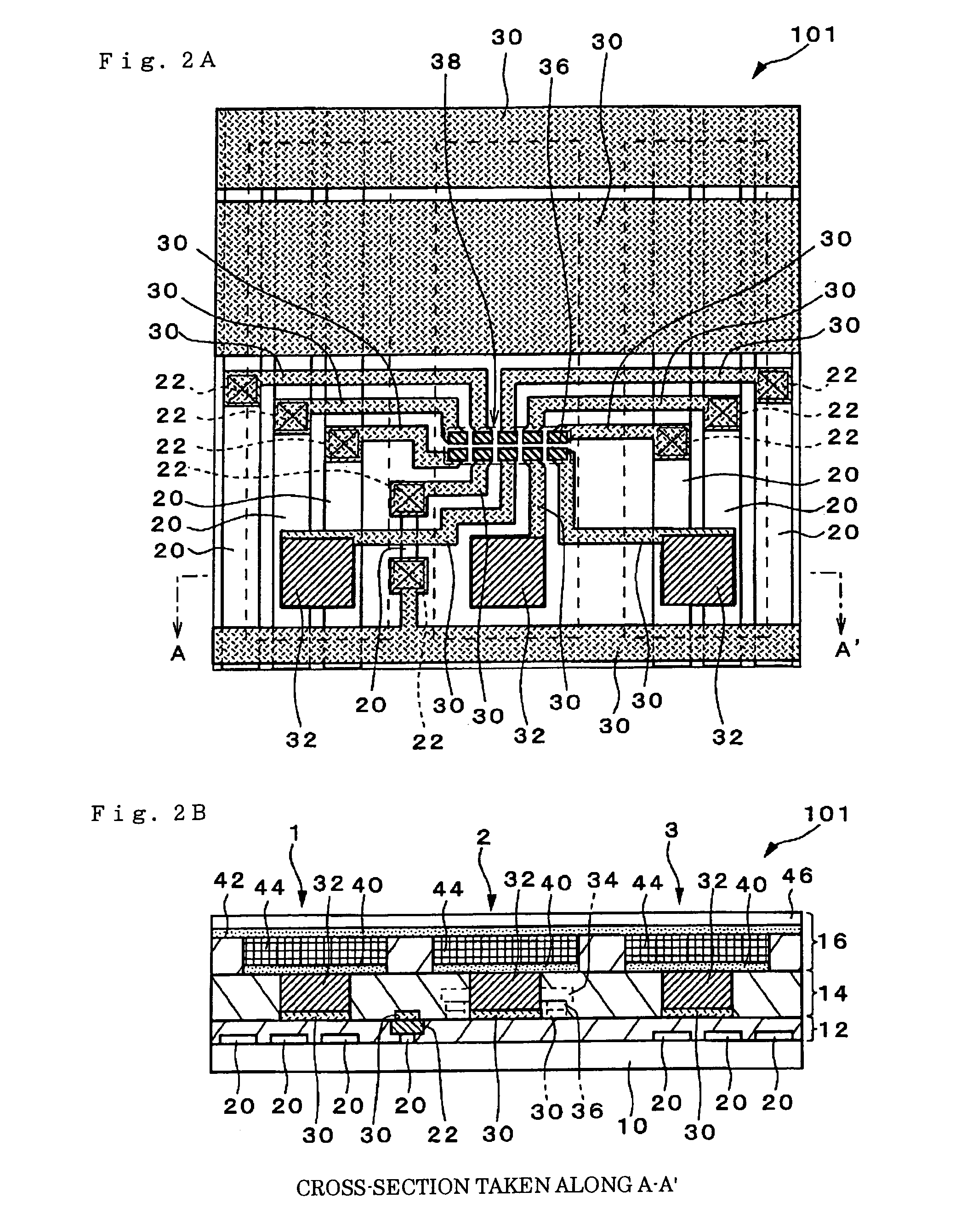
[0046]FIG


PUM


Abstract

The invention enhances a production yield of a display device (an electro-optical device). The invention provides a method of manufacturing an electro-optical device including a display region in which a plurality of basic pixels are arranged, each basic pixel including a plurality of color pixels. The method includes: forming on a first substrate lines to drive a plurality of electro-optical elements respectively constituting the color pixels, correspondingly to the arrangement of the basic pixels; forming on a second substrate, as a chip to be transferred to each basic pixel, a drive circuit to drive the plurality of electro-optical elements which constitutes the plurality of color pixels of the basic pixels to obtain a plurality of basic-pixel driving chips; and transferring step of transferring the respective basic-pixel driving chips from the second substrate onto the first substrate, and connecting the drive circuits to regions of the lines corresponding to the basic pixels.

Description


Claims


Application Information

Patent Timeline
Owner SEIKO EPSON CORP
Why Eureka
Try Eureka