Semiconductor light-emitting device and method for fabricating the same
- Summary
- Abstract
- Description
- Claims
- Application Information
AI Technical Summary
Benefits of technology
Problems solved by technology
Method used
Image

Examples
embodiment 1
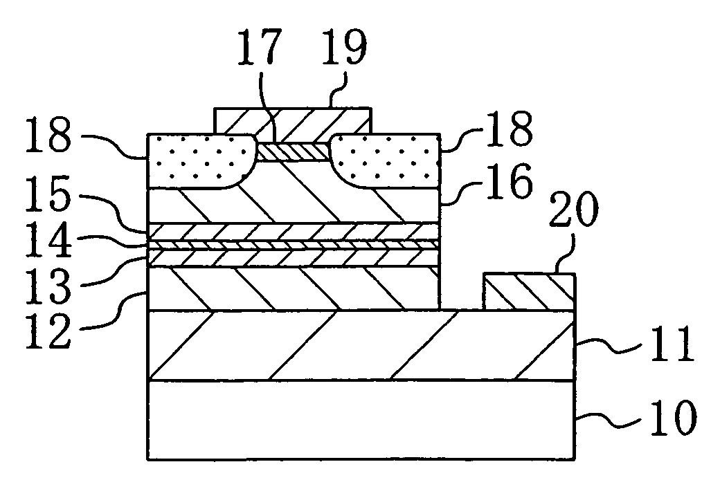
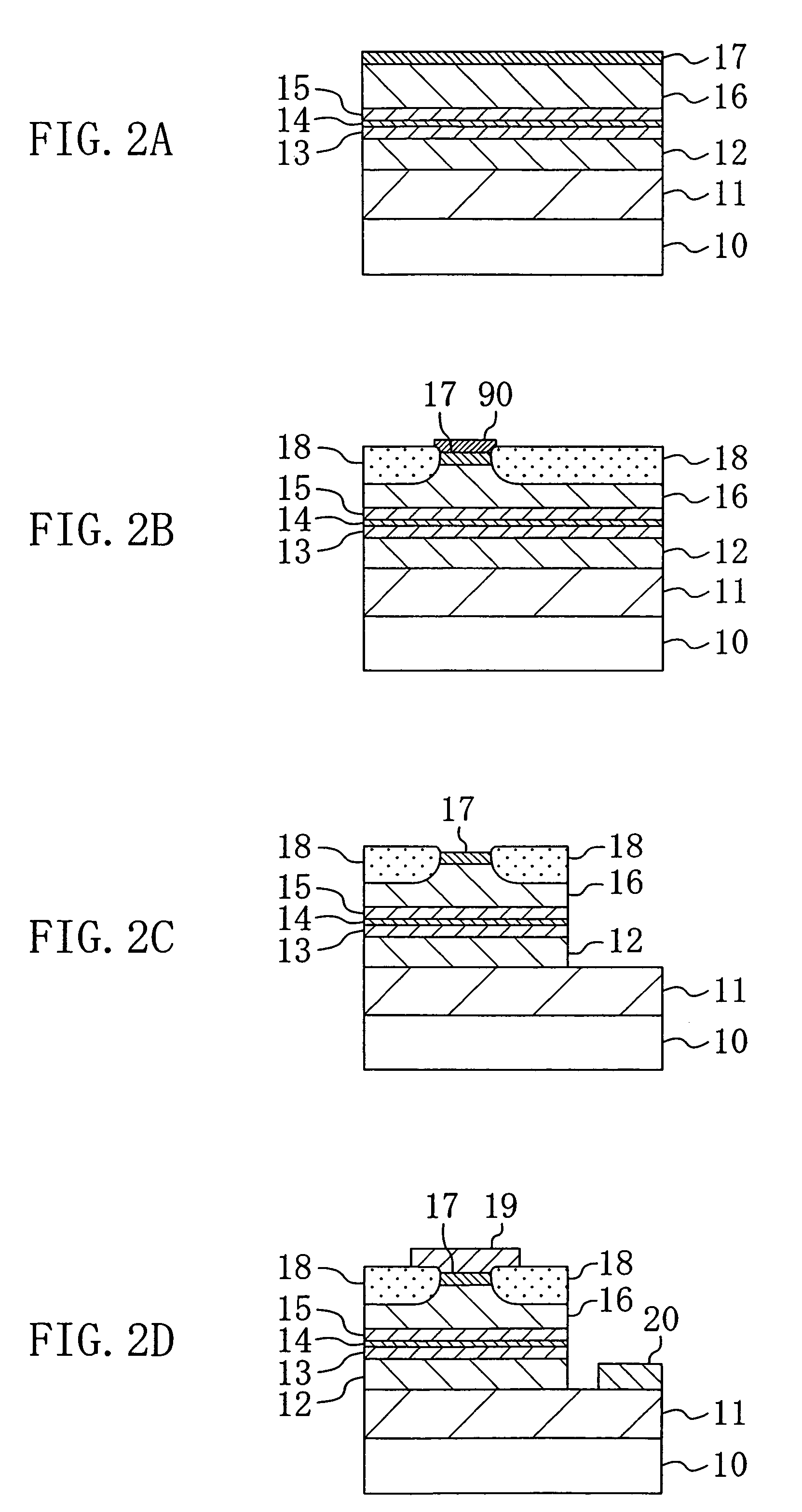
[0036]A first embodiment of the present invention will be described with reference to the drawings.
[0037]FIG. 1 shows a cross-sectional structure of a semiconductor laser device according to the first embodiment.
[0038]The semiconductor laser device shown in FIG. 1 has a double heterostructure including cladding layers composed of an aluminum gallium nitride (AlGaN) having a relatively large band gap and a quantum well layer and the like composed of any of a gallium nitride (GaN), a gallium indium nitride (GaInN) and a combination thereof each having a band gap smaller than that of the cladding layers, which are sandwiched between the cladding layers. A description will be given herein below to the case where a single quantum well separate confinement heterostructure (SQW-SCH) is used.
[0039]As shown in FIG. 1, an n-type buffer layer 11 composed of n-type GaN with a thickness of about 2 μm, an n-type cladding layer 12 composed of n-type Al0.15Ga0.85N with a thickness of about 1 μm, an n-
embodiment 2
[0071]A second embodiment of the present invention will be described herein below with reference to the drawings.
[0072]FIG. 8 shows a cross-sectional structure of a semiconductor laser device according to the second embodiment.
[0073]In contrast to the first embodiment which uses insulating sapphire to compose the substrate 10 on which the epitaxial layer is grown, the second embodiment uses, to compose a substrate 30, any of an n-type gallium nitride (GaN), an n-type aluminum gallium nitride (AlGaN), and an n-type silicon carbide (SiC) each having conductivity and close in lattice constant to a Group III nitride semiconductor, as shown in FIG. 8.
[0074]As shown in FIG. 8, an n-type buffer layer 31 composed of n-type GaN with a thickness of about 2 μm, an n-type cladding layer 32 composed of n-type Al0.15Ga0.85N with a thickness of about 1 μm, an n-type optical confinement layer 33 composed of n-type GaN with a thickness of about 0.1 μm, a single quantum well active layer 34 composed of
embodiment 3
[0088]A third embodiment of the present invention will be described herein below with reference to the drawings.
[0089]FIG. 10 shows a cross-sectional structure of a semiconductor laser device according to the third embodiment.
[0090]A structure according to the third embodiment is obtainable by further improving the light confining efficiency of the ridge structure of the semiconductor laser device described in the second embodiment.
[0091]As shown in FIG. 10, an n-type buffer layer 51 composed of n-type GaN with a thickness of about 2 μm, an n-type cladding layer 52 composed of n-type Al0.15Ga0.85N with a thickness of about 1 μm, an n-type optical confinement layer 53 composed of n-type GaN with a thickness of about 0.1 μm, a single quantum well active layer 54 composed of undoped Ga0.8In0.2N with a thickness of about 5 μnm, a p-type optical confinement layer 55 composed of p-type GaN with a thickness of about 0.1 μm, a p-type cladding layer 56 composed of p-type Al0.15Ga0.85N with a th
PUM
 Abstract
Description
Claims
Application Information
 - R&D Engineer
- R&D Manager
- IP Professional
- Industry Leading Data Capabilities
- Powerful AI technology
- Patent DNA Extraction
Browse by: Latest US Patents, China's latest patents, Technical Efficacy Thesaurus, Application Domain, Technology Topic.
© 2024 PatSnap. All rights reserved.Legal|Privacy policy|Modern Slavery Act Transparency Statement|Sitemap