Process for pressing galvanized PCB boards and multi-layer PCB board

A PCB board and process technology, which is applied in the lamination process and multi-layer PCB board field, can solve the problems of PCB board short circuit, waste of processing resources, easy copper penetration, etc., and achieve the effect of preventing glue shortage and avoiding waste of processing resources

Inactive Publication Date: 2010-05-19
SHENNAN CIRCUITS
View PDF0 Cites 12 Cited by
  • Summary
  • Abstract
  • Description
  • Claims
  • Application Information

AI Technical Summary

Benefits of technology

This technology helps protect electronic components from damage during manufacturing processes such as soldering or reflow. It involves applying an adhesive called epoxy resin onto one side of each line (or wire) before inserting it inside another part that needs them for electrical connection). By doing this, they can be securely fixed together with no excess material being left behind after creation.

Problems solved by technology

The technical problem addressed by this patented technology relates to improving the quality of multilevel printed wiring boards during production due to defects caused by insufficient filling of gaps with resin when repeatedly used over multiple layers without leaving any residues behind. This issue affects both signal transmission speed and reliability of electronic devices made from these circuits.

Method used


Image

  • Process for pressing galvanized PCB boards and multi-layer PCB board
  • Process for pressing galvanized PCB boards and multi-layer PCB board
  • Process for pressing galvanized PCB boards and multi-layer PCB board

Examples


Embodiment Construction

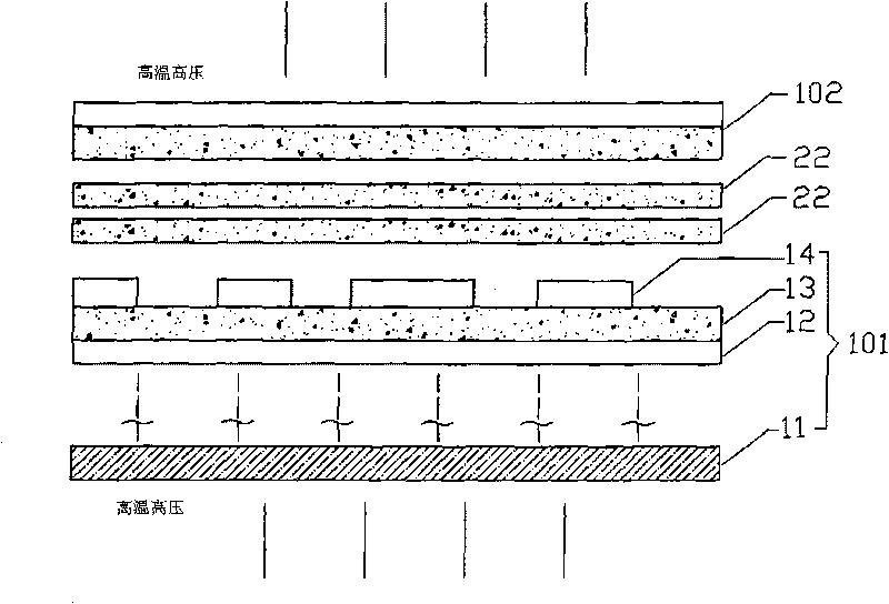
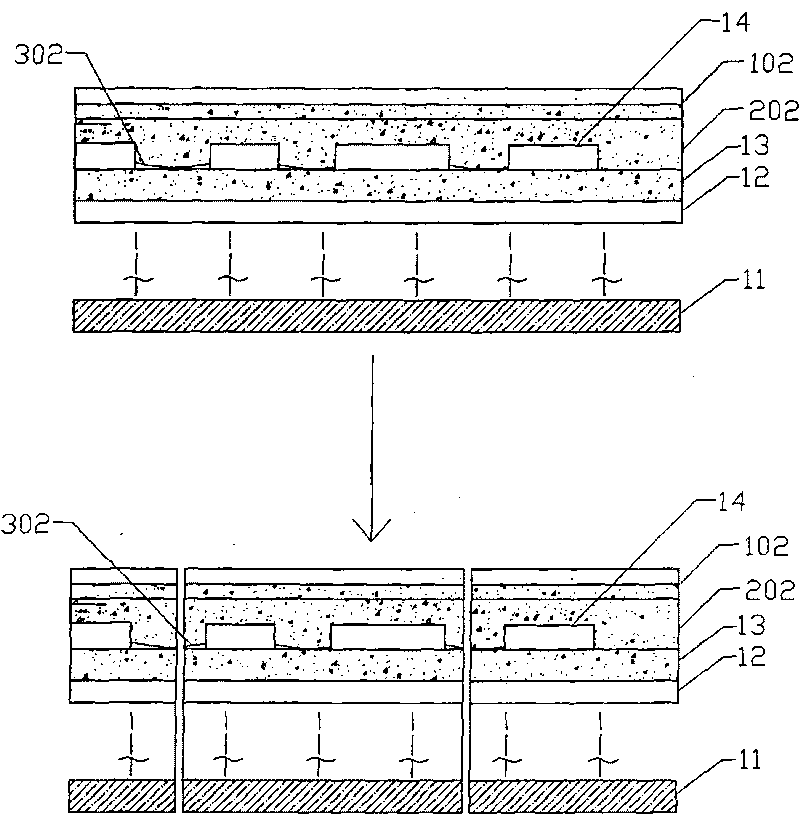
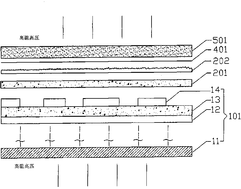
[0020] Refer below Figure 3-Figure 6 An embodiment of the lamination process after electroplating of the PCB provided by the present invention is described in detail.

[0021] In this embodiment, the sequential pressing process mainly includes the following steps:

[0022] refer to image 3 , in the first pressing step, after the lower core board assembly 101 to be pressed is sequentially covered with a layer of insulating leakage trap 201, a layer of spacer 301, and a layer of heat-resistant and pressure-resistant elastic gasket 501, the Under the condition of high temperature and high pressure, the lower core board assembly 101 and the upper layer core board assembly 102 are pressed together, and the adhesive sheet 301 is pressed into the groove 14 between the copper foil lines on the surface of the lower core board assembly 101. The deformation of the pressure-resistant elastic gasket 501 can press the insulating leak trap 201 into the groove between the copper foil lines 1


PUM


Abstract

The invention discloses a process for pressing galvanized PCB boards. The process comprises the following steps of: the first pressing step, after sequentially covering a bonding sheet, a copper foil and an elastic pad on a core board assembly to be pressed, pressing the core board assembly under the high-temperature and high-pressure condition, and pressing the bonding sheet into grooves among copper foil lines on the surface of the core board assembly; the copper removing step, after detaching the silica gel pad, removing the overlaid copper foil to expose the cured bonding sheet; and the second pressing step, after covering another bonding sheet on the semi-finished product of which an insulating sheet is removed, pressing the bonding sheet and the core board assembly to be pressed with the bonding sheet under the high-temperature and high-pressure condition. The invention also discloses a corresponding multi-layer PCB board. The invention can effectively prevent the gel shortage problem due to the excessive thickness of inner-layer copper foil lines after pressing and various quality problems caused by gel shortage, and avoids the waste of processing resources in subsequent procedures as a result of gel shortage.

Description


Claims


Application Information

Patent Timeline
Owner SHENNAN CIRCUITS
Why Eureka
Try Eureka