Method for manufacturing flash memory

A manufacturing method and memory technology, which is applied in semiconductor/solid-state device manufacturing, electrical components, circuits, etc., can solve the problems of difficult etching process, etc., and achieve the effect of maintaining integrity and increasing contact area

Active Publication Date: 2010-12-22
WINBOND ELECTRONICS CORP
View PDF0 Cites 11 Cited by
  • Summary
  • Abstract
  • Description
  • Claims
  • Application Information

AI Technical Summary

Benefits of technology

This patented technology allows for better performance by increasing the number of transistors within each cell without compromising their ability to switch data effectively or withstand damage caused during programming operations. By covering certain areas around it instead of removing them entirely from the chip design, there are fewer steps needed when creating these memories compared to traditional methods like adding layers afterwards. Additionally, this process helps maintain the quality of the surrounding material while also improving its overall effectiveness over time.

Problems solved by technology

This patented technical solution involves optimizing removal of certain parts or layers within non volatile memories that have different levels of capacitance across their entirety. These areas include both the active regions where programming operations occur during normal operation but also other areas such as the surrounding circuitry around them called the boundary conditions. Additionally, there should ideality be provided for efficient manufacturing processes while ensuring proper alignment among these various materials when they come together.

Method used


Image

  • Method for manufacturing flash memory
  • Method for manufacturing flash memory
  • Method for manufacturing flash memory

Examples


no. 1 example

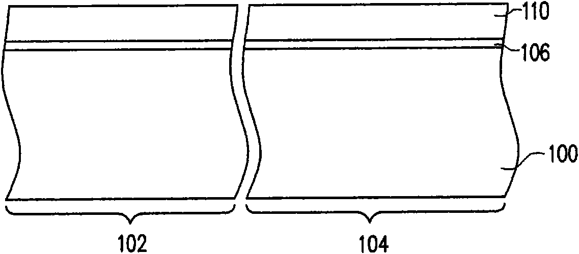
[0033] Figure 1A to Figure 1I is a schematic cross-sectional flow diagram of a method for manufacturing a flash memory according to the first embodiment of the present invention.

[0034] Please refer to Figure 1A , firstly, a substrate 100 is provided. The substrate 100 is, for example, a silicon substrate. The substrate 100 includes a memory area 102 and a peripheral area 104 . Then, a first dielectric layer 106 and a mask layer 110 are sequentially formed on the substrate 100 . The material of the first dielectric layer 106 is, for example, silicon oxide, and its formation method is, for example, thermal oxidation or chemical vapor deposition. The material of the mask layer 110 is, for example, silicon nitride, and its formation method is, for example, chemical vapor deposition.

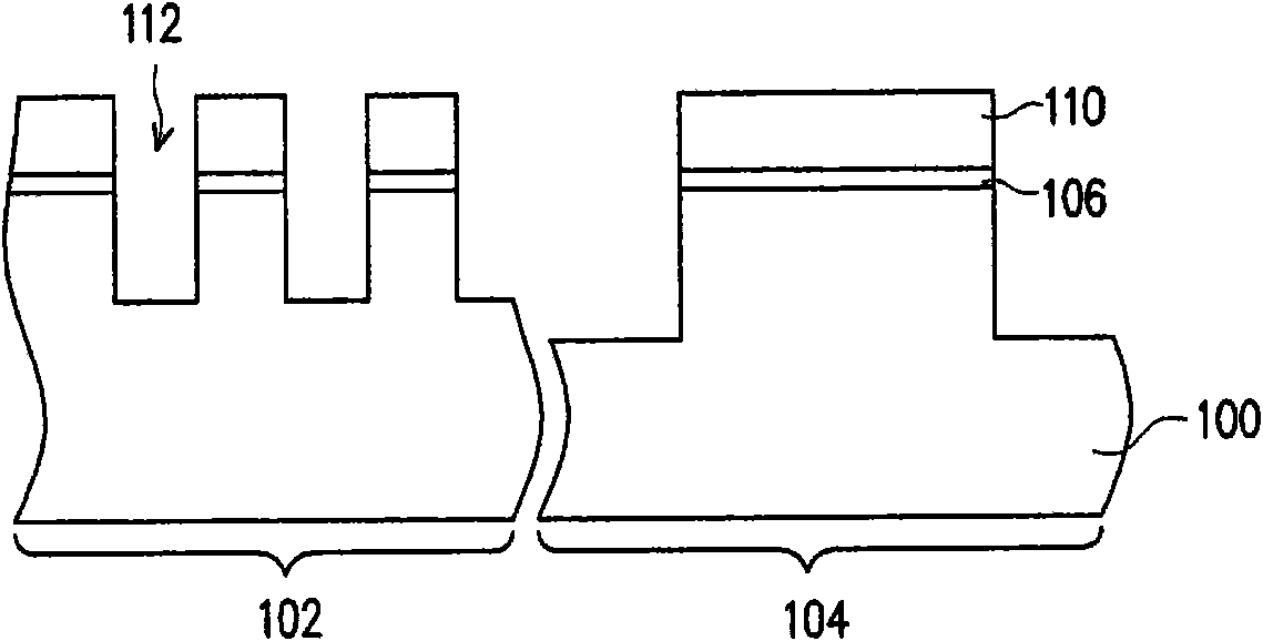
[0035] Please refer to Figure 1B , and then, removing part of the mask layer 110 , the first dielectric layer 106 and the substrate 100 to form the trench 112 . A method for removing part of

no. 2 example

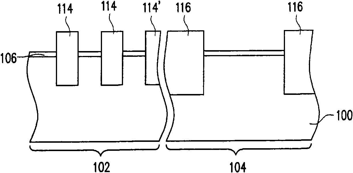
[0046] Figure 2A to Figure 2C It is a schematic cross-sectional flow diagram of a part of a manufacturing method of a flash memory according to the second embodiment of the present invention. In this embodiment, the front-end process of the flash memory is the same as that in the first embodiment Figure 1A to Figure 1D and its corresponding instructions are similar, so the following is only for the continuation Figure 1D steps are explained.

[0047] Please also refer to Figure 1D and Figure 2A After the stacked tunneling dielectric layer 108 and the floating gate 120 are formed on the substrate 100 between the isolation structures 114, 114', 116, for example, the isolation structures 114, 114', 116 are blanketed ) are removed to form isolation structures 114a, 114'a, 116a. Wherein, the surfaces 124, 125, 126 of the isolation structures 114a, 114'a, 116a are higher than the surface 109 of the tunnel dielectric layer 108, and the surfaces 124, 125, 126 of the isolation s


PUM


Abstract

The invention provides a method for manufacturing a flash memory. The method comprises the following steps of: providing a substrate, wherein a plurality of isolation structures are arranged on the substrate, and a dielectric layer and a floating gate are arranged on the substrate among the isolation structures; forming a mask layer on the substrate to cover the isolation structures in a peripheral area and the isolation structures which are positioned in a memory area and are adjacent to the peripheral area; removing one part of the isolation structures in the memory area by taking the mask layer as a mask, so that the first height difference between the surfaces of the isolation structures in the peripheral area and the surface of the dielectric layer and between the surfaces of the isolation structures which are positioned in the memory area and are adjacent to the peripheral area and the surface of the dielectric layer exists, and the second height difference which is less than first height difference exists between the surfaces of the rest isolation structures in the memory area and the surface of the dielectric layer; removing the mask layer; forming a gate dielectric layer on the substrate; and forming a conductor layer on the substrate. The flash memory manufactured by the method has high-grid coupling efficiency and excellent electrical property.

Description


Claims


Application Information

Patent Timeline
Owner WINBOND ELECTRONICS CORP
Why Eureka
Try Eureka