Flash memory management method and flash memory device

A technology of flash memory management and flash memory, which is applied in the field of flash memory management methods and flash memory devices, can solve problems such as affecting the efficiency of writing data, slow data writing speed, and limited erasing times of flash memory blocks, so as to reduce copying, moving operations and erasing operation, improve write speed, and reduce memory usage

Active Publication Date: 2012-12-26
SHENZHEN NETCOM ELECTRONICS CO LTD
View PDF7 Cites 27 Cited by
  • Summary
  • Abstract
  • Description
  • Claims
  • Application Information

AI Technical Summary

Problems solved by technology

Since the temporary blocks reserved in the flash memory are limited, in a system with frequent random writes, it is necessary to continuously perform data copying, moving and block erasing operations, which greatly affects the efficiency of writing data
[0005] To sum up, in the existing block-based flash memory management method, in a system with frequent random writes and discontinuous random write addresses, due to the continuous operation of copying and moving data and erasing blocks, this will cause data The problem of slow writing speed, and because the erasing times of each flash memory block is limited, when the erasing times of a flash memory block reaches its service life, the performance of the flash memory device will be greatly reduced, thus affecting the use of the flash memory device life

Method used


Image

  • Flash memory management method and flash memory device
  • Flash memory management method and flash memory device
  • Flash memory management method and flash memory device

Examples


Embodiment Construction

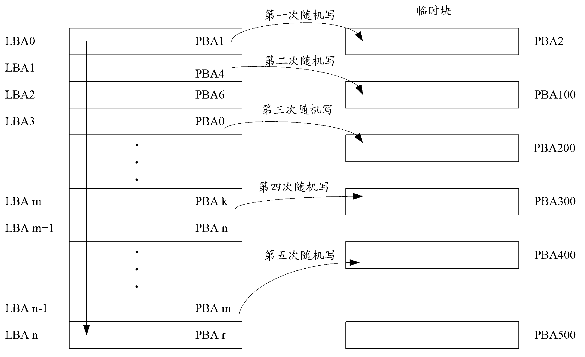
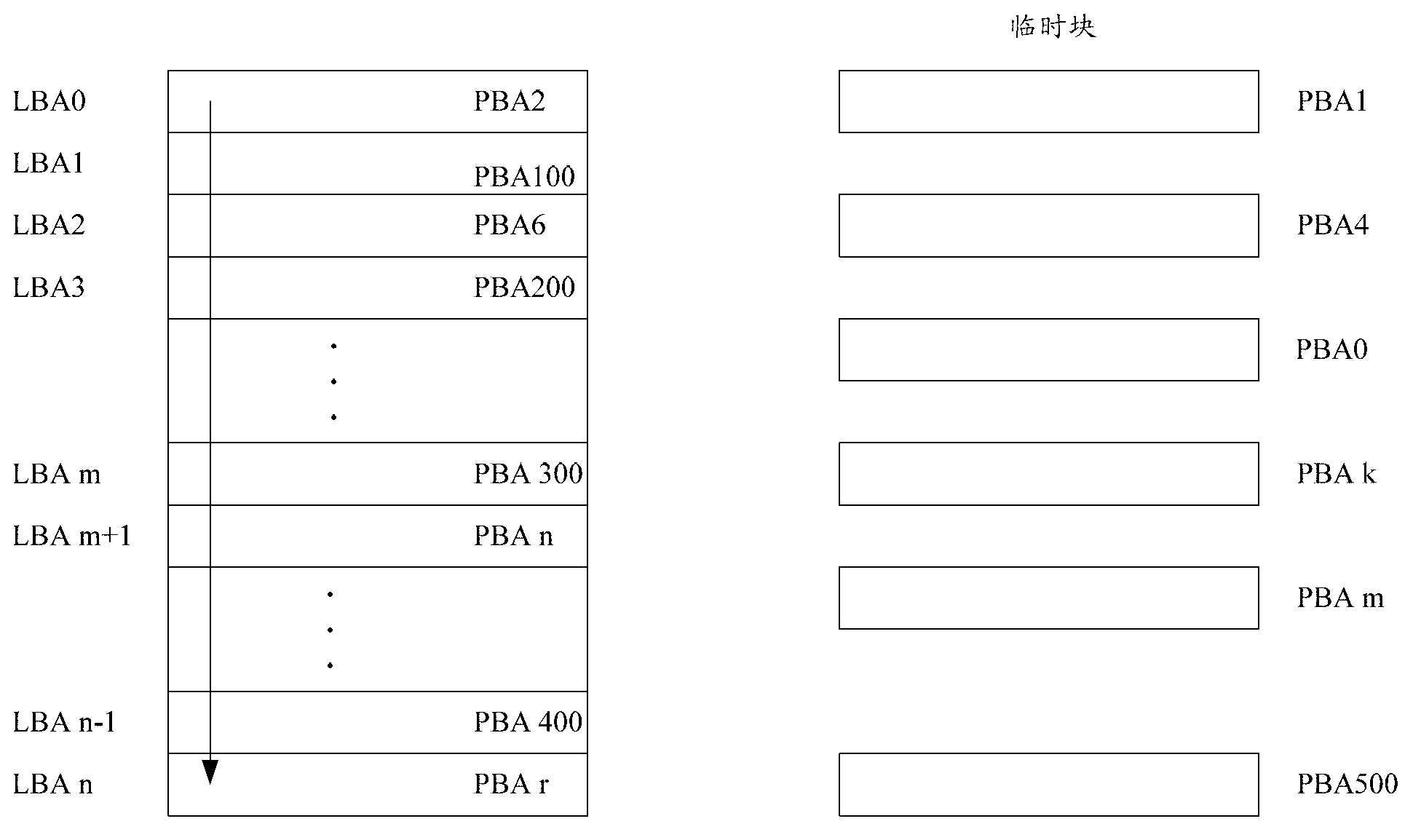
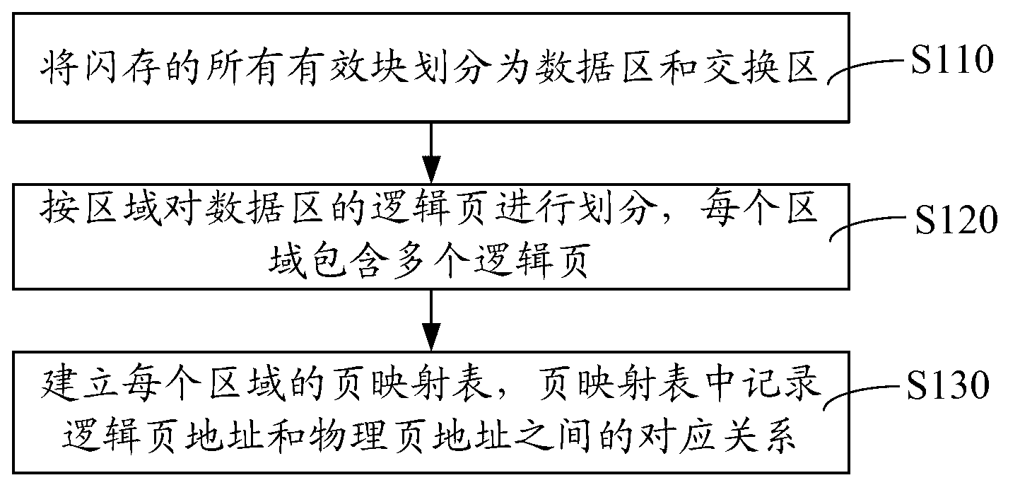
[0062] The flash memory management method and the technical solution of the flash memory device will be described in detail below in conjunction with specific embodiments and accompanying drawings, so as to make it more clear.

[0063] Such as figure 2 Shown, in one embodiment, a kind of flash memory management method comprises the following steps:

[0064] Step S110, dividing all valid blocks of the flash memory into a data area and a swap area.

[0065] Specifically, at least two valid blocks (blocks) are set in the swap area. The more effective blocks are set in the swap area, the more conducive to the global balance wear of the flash memory, but the storage space of the data area will be relatively smaller.

[0066] In step S120, the logical pages of the data area are divided into areas, and each area includes multiple logical pages.

[0067] Specifically, each valid block includes multiple logical pages. Divide the logical pages of the data area into regions, such as ...


PUM


Abstract

The invention relates to a flash memory management method and a flash memory device. The flash memory management method comprises following steps of dividing all active blocks of a flash memory into a data area and a switching area; dividing a logical page of the data area according to the area, wherein each area comprises a plurality of logical pages; and establishing a page mapping table of each area, and recording a correspondence relation of a logical page address and a physical page address in the page mapping table. According to the flash memory management method and the flash memory device, the data area of the flash memory is divided into different areas, the page mapping table of each area is established, the correspondence relation of the logical page address and the physical page address is recorded in the page mapping table, the flash memory is managed by adopting the page as a unit, when data is written in the flash memory, the data can be written into the flash memory according to the page sequence, after multiple pages of one block are fulfilled, the data is written into a next empty block, the utilization rate of the block is improved, the copy moving operation and erasing operation of the data can be reduced, the writing-in speed of the flash memory is improved, and the occupation of an internal memory can be reduced by establishing the page mapping table according to the areas.

Description

technical field [0001] The invention relates to a storage device, in particular to a flash memory management method and a flash memory device. Background technique [0002] Flash memory is a semiconductor-based memory that has the advantages of low power consumption, large capacity, high access speed, no mechanical failure, and data non-volatility. With the rapid growth of flash memory storage capacity, people put forward higher and higher requirements for the flexibility of data operation, and the management of data storage in flash memory has become an unavoidable problem. [0003] Flash memory, especially NAND Flash, has been widely used in mobile storage devices, such as U disk, SD (Secure Digital Memory Card) card, SSD (Solid State Disk) solid state drive, etc. Due to the characteristics of flash memory, the same page cannot be reprogrammed, and the entire block must be erased before programming (programming is data writing). However, when erasing a block, the valid da...

Claims


Application Information

Patent Timeline
IPC IPC(8): G06F12/02
Inventor 尹慧李志雄邓恩华
Owner SHENZHEN NETCOM ELECTRONICS CO LTD
Why Eureka
Try Eureka