Glue overflow preventing technique for PCB packaging process
A kind of PCB board, anti-overflow glue technology, applied in the direction of electrical components, circuits, semiconductor devices, etc., can solve the problems of enterprise trouble, unusable, packaging glue overflowing into the hole ring of the circuit board, etc., to achieve the best technical effect, good sealing sexual effect
- Summary
- Abstract
- Description
- Claims
- Application Information
AI Technical Summary
Problems solved by technology
Method used
Image

Examples
Example Embodiment
[0029] Examples:
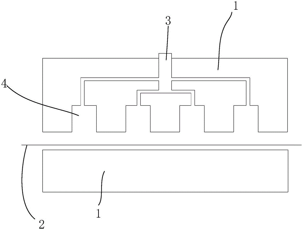
[0030] The embodiment of the present invention provides an anti-overflow glue process in the PCB board packaging process, such as figure 1 , figure 2 As shown, the anti-overflow glue process of the PCB board packaging process includes the use of a glue injection mold 1. The glue injection mold 1 is provided with a glue runner 3 for glue injection, and the glue is on the PCB board 2. The glue guide groove 4 with surface flow forming, the process includes the following steps:
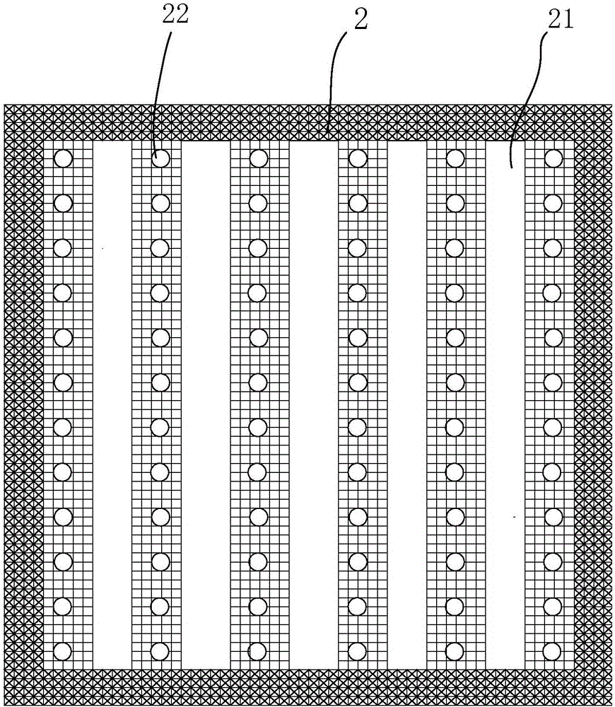
[0031] Step 1: Place the PCB board 2 on the glue injection mold 1 and adjust the relative position of the glue injection mold 2 and the PCB board 2 to ensure that the position of the glue guide groove 4 does not cover the hole ring 22 on the PCB board. Prevent the glue in the glue guide groove 4 from overflowing into the orifice ring 22;
[0032] Step 2: Close the injection mold 1 in Step 1, adjust the pressure on the injection mold 1 to 25-50 kg, heat the injection mold 1 to 140°C to 170°C, an
PUM
 Abstract
Description
Claims
Application Information
 - R&D Engineer
- R&D Manager
- IP Professional
- Industry Leading Data Capabilities
- Powerful AI technology
- Patent DNA Extraction
Browse by: Latest US Patents, China's latest patents, Technical Efficacy Thesaurus, Application Domain, Technology Topic.
© 2024 PatSnap. All rights reserved.Legal|Privacy policy|Modern Slavery Act Transparency Statement|Sitemap